PIC18F2450/4450
13.0 CAPTURE/COMPARE/PWM
(CCP) MODULE
PIC18F2450/4450 devices have one CCP (Capture/
Compare/PWM) module. The module contains a 16-bit
register, which can operate as a 16-bit Capture register,
a 16-bit Compare register or a PWM Master/Slave Duty
Cycle register.
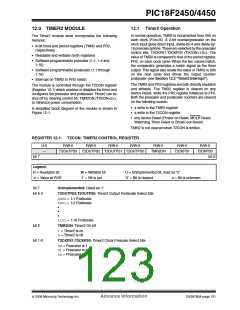
REGISTER 13-1: CCP1CON: CAPTURE/COMPARE/PWM CONTROL REGISTER
U-0
—
U-0
—
R/W-0
R/W-0
R/W-0
R/W-0
R/W-0
R/W-0
DC1B1
DC1B0
CCP1M3
CCP1M2
CCP1M1
CCP1M0
bit 7
bit 0
Legend:
R = Readable bit
-n = Value at POR
W = Writable bit
‘1’ = Bit is set
U = Unimplemented bit, read as ‘0’
‘0’ = Bit is cleared x = Bit is unknown
bit 7-6
bit 5-4
Unimplemented: Read as ‘0’
DC1B1:DC1B0: PWM Duty Cycle for CCP Module bits
Capture mode:
Unused.
Compare mode:
Unused.
PWM mode:
These bits are the two LSbs (bit 1 and bit 0) of the 10-bit PWM duty cycle. The eight MSbs of the duty
cycle are found in CCPR1L.
bit 3-0
CCP1M3:CCP1M0: CCP Module Mode Select bits
0000= Capture/Compare/PWM disabled (resets CCP module)
0001= Reserved
0010= Compare mode: toggle output on match (CCP1IF bit is set)
0011= Reserved
0100= Capture mode: every falling edge
0101= Capture mode: every rising edge
0110= Capture mode: every 4th rising edge
0111= Capture mode: every 16th rising edge
1000= Compare mode: initialize CCP1 pin low; on compare match, force CCP1 pin high
(CCP1IF bit is set)
1001= Compare mode: initialize CCP1 pin high; on compare match, force CCP1 pin low
(CCP1IF bit is set)
1010= Compare mode: generate software interrupt on compare match (CCP1IF bit is set,
CCP1 pin reflects I/O state)
1011= Compare mode: trigger special event, reset timer and start A/D conversion on CCP1 match
(CCP1IF bit is set)
11xx= PWM mode
© 2006 Microchip Technology Inc.
Advance Information
DS39760A-page 123

 MICROCHIP [ MICROCHIP ]