PIC18F2450/4450
12.1 Timer2 Operation
12.0 TIMER2 MODULE
In normal operation, TMR2 is incremented from 00h on
each clock (FOSC/4). A 2-bit counter/prescaler on the
clock input gives direct input, divide-by-4 and divide-by-
16 prescale options. These are selected by the prescaler
control bits, T2CKPS1:T2CKPS0 (T2CON<1:0>). The
value of TMR2 is compared to that of the period register,
PR2, on each clock cycle. When the two values match,
the comparator generates a match signal as the timer
output. This signal also resets the value of TMR2 to 00h
on the next cycle and drives the output counter/
postscaler (see Section 12.2 “Timer2 Interrupt”).
The Timer2 module timer incorporates the following
features:
• 8-bit timer and period registers (TMR2 and PR2,
respectively)
• Readable and writable (both registers)
• Software programmable prescaler (1:1, 1:4 and
1:16)
• Software programmable postscaler (1:1 through
1:16)
• Interrupt on TMR2 to PR2 match
The TMR2 and PR2 registers are both directly readable
and writable. The TMR2 register is cleared on any
device Reset, while the PR2 register initializes at FFh.
Both the prescaler and postscaler counters are cleared
on the following events:
The module is controlled through the T2CON register
(Register 12-1) which enables or disables the timer and
configures the prescaler and postscaler. Timer2 can be
shut off by clearing control bit, TMR2ON (T2CON<2>),
to minimize power consumption.
• a write to the TMR2 register
• a write to the T2CON register
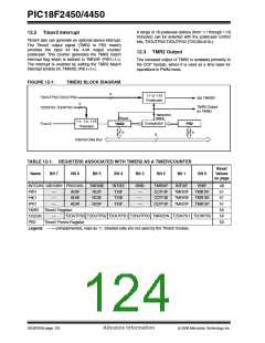
A simplified block diagram of the module is shown in
Figure 12-1.
• any device Reset (Power-on Reset, MCLR Reset,
Watchdog Timer Reset or Brown-out Reset)
TMR2 is not cleared when T2CON is written.
REGISTER 12-1: T2CON: TIMER2 CONTROL REGISTER
U-0
—
R/W-0
R/W-0
R/W-0
R/W-0
R/W-0
R/W-0
R/W-0
T2OUTPS3 T2OUTPS2 T2OUTPS1 T2OUTPS0
TMR2ON
T2CKPS1
T2CKPS0
bit 7
bit 0
Legend:
R = Readable bit
-n = Value at POR
W = Writable bit
‘1’ = Bit is set
U = Unimplemented bit, read as ‘0’
‘0’ = Bit is cleared x = Bit is unknown
bit 7
Unimplemented: Read as ‘0’
bit 6-3
T2OUTPS3:T2OUTPS0: Timer2 Output Postscale Select bits
0000= 1:1 Postscale
0001= 1:2 Postscale
•
•
•
1111= 1:16 Postscale
bit 2
TMR2ON: Timer2 On bit
1= Timer2 is on
0= Timer2 is off
bit 1-0
T2CKPS1:T2CKPS0: Timer2 Clock Prescale Select bits
00= Prescaler is 1
01= Prescaler is 4
1x= Prescaler is 16
© 2006 Microchip Technology Inc.
Advance Information
DS39760A-page 121

 MICROCHIP [ MICROCHIP ]