PIC18CXX2
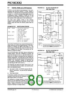
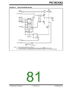
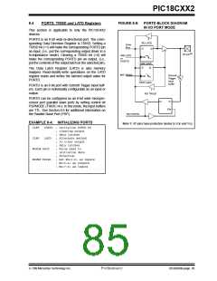
FIGURE 8-6: BLOCK DIAGRAM OF RB3
VDD
RBPU(2)
weak
pull-up
P
CCP2MX
CCP Output(3)
1
0
VDD
P
Enable (3)
CCP Output
Data Latch
I/O
Data Bus
D
Q
Pin(1)
WR LATB or
WR PORTB
N
CK
TRIS Latch
D
VSS
TTL
WR TRISB
Input
CK
Q
Buffer
RD TRISB
RD LATB
D
Q
EN
RD PORTB
RD PORTB
CCP2 input(3)
Schmitt Trigger
Buffer
CCP2MX = 0
Note 1: I/O pin has diode protection to VDD and VSS.
2: To enable weak pull-ups, set the appropriate DDR bit(s) and clear the RBPU bit (INTCON2<7>).
3: The CCP2 input/output is multiplexed with RB3 if the CCP2MX bit is enabled (=’0’) in the configuration register.
7/99 Microchip Technology Inc.
Preliminary
DS39026B-page 81

 MICROCHIP [ MICROCHIP ]