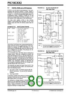
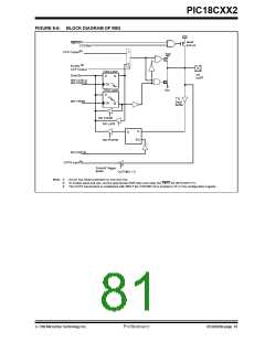
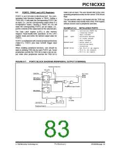
PIC18CXX2
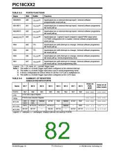
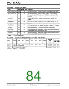
TABLE 8-5:
Name
PORTC FUNCTIONS
Bit# Buffer Type
Function
RC0/T1OSO/T1CKI
RC1/T1OSI/CCP2
bit0
bit1
ST
ST
Input/output port pin or Timer1 oscillator output/Timer1 clock input
Input/output port pin, Timer1 oscillator input, or Capture2 input/
Compare2 output/PWM output when CCP2MX configuration bit is
disabled.
RC2/CCP1
bit2
bit3
ST
ST
Input/output port pin or Capture1 input/Compare1 output/PWM1
output
RC3 can also be the synchronous serial clock for both SPI and I2C
modes.
RC3/SCK/SCL
RC4 can also be the SPI Data In (SPI mode) or data I/O (I2C mode).
Input/output port pin or Synchronous Serial Port data output
RC4/SDI/SDA
bit4
ST
RC5/SDO
bit5
bit6
ST
ST
RC6/TX/CK
Input/output port pin, Addressable USART Asynchronous Transmit, or
Addressable USART Synchronous Clock
RC7/RX/DT
bit7
ST
Input/output port pin, Addressable USART Asynchronous Receive, or
Addressable USART Synchronous Data
Legend: ST = Schmitt Trigger input
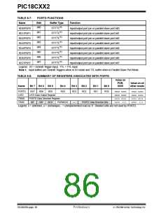
TABLE 8-6:
Name
SUMMARY OF REGISTERS ASSOCIATED WITH PORTC
Value on
POR,
BOR
Value on all
other resets
Bit 7
Bit 6
Bit 5
Bit 4
Bit 3
Bit 2
Bit 1
Bit 0
PORTC
LATC
RC7
RC6
RC5
RC4
RC3
RC2
RC1
RC0
xxxx xxxx
xxxx xxxx
1111 1111
uuuu uuuu
uuuu uuuu
1111 1111
LATC Data Output Register
TRISC
PORTC Data Direction Register
Legend: x = unknown, u = unchanged.
DS39026B-page 84
Preliminary
7/99 Microchip Technology Inc.

 MICROCHIP [ MICROCHIP ]