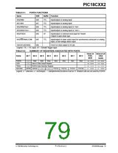
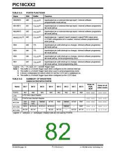
PIC18CXX2
make a pin an input. The user should refer to the corre-
sponding peripheral section for the correct TRIS bit set-
tings.
8.3
PORTC, TRISC and LATC Registers
PORTC is an 8 bit wide bi-directional port. The corre-
sponding Data Direction Register is TRISC. Setting a
TRISC bit (=1) will make the corresponding PORTC pin
an input, (i.e., put the corresponding output driver in a
hi-impedance mode). Clearing a TRISC bit (=0) will
make the corresponding PORTC pin an output, (i.e.,
put the contents of the output latch on the selected pin).
The pin override value is not loaded into the TRIS reg-
ister. This allows read-modify-write of the TRIS register,
without concern due to peripheral overrides.
EXAMPLE 8-3: INITIALIZING PORTC
CLRF
PORTC
; Initialize PORTC by
; clearing output
; data latches
The Data Latch register (LATC) is also memory
mapped. Read-modify-write operations on the LATC
register reads and writes the latched output value for
PORTC.
CLRF
LATC
; Alternate method
; to clear output
; data latches
PORTC is multiplexed with several peripheral functions
(Table 8-5). PORTC pins have Schmitt Trigger input
buffers.
MOVLW 0xCF
; Value used to
; initialize data
; direction
MOVWF TRISC
; Set RC<3:0> as inputs
; RC<5:4> as outputs
; RC<7:6> as inputs
When enabling peripheral functions, care should be
taken in defining TRIS bits for each PORTC pin. Some
peripherals override the TRIS bit to make a pin an out-
put, while other peripherals override the TRIS bit to
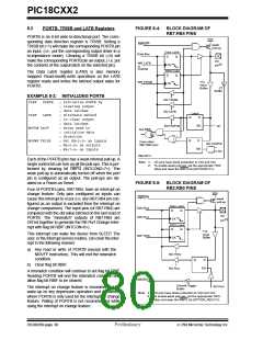
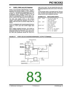
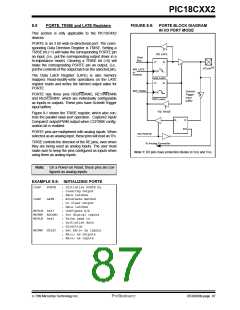
FIGURE 8-7: PORTC BLOCK DIAGRAM (PERIPHERAL OUTPUT OVERRIDE)
Peripheral Data Out
RD LATC
Data Bus
1
RC7: RC0
D
Q
Q
WR LATC or
WR PORTC
0
CK
Peripheral Out
Select
RD TRISC
Peripheral Output Enable
D
Q
Q
WR TRISC
CK
Q
Q
D
ST Buffer
CK
RD PORTC
Peripheral Data In
7/99 Microchip Technology Inc.
Preliminary
DS39026B-page 83

 MICROCHIP [ MICROCHIP ]