PIC18CXX2
8.2
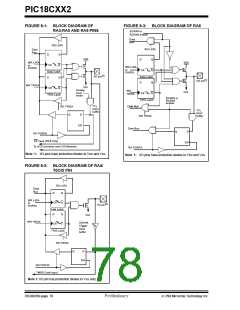
PORTB, TRISB and LATB Registers
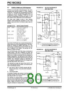
FIGURE 8-4: BLOCK DIAGRAM OF
RB7:RB4 PINS
PORTB is an 8-bit wide bi-directional port. The corre-
sponding data direction register is TRISB. Setting a
TRISB bit (=1) will make the corresponding PORTB pin
an input, (i.e., put the corresponding output driver in a
hi-impedance mode). Clearing a TRISB bit (=0) will
make the corresponding PORTB pin an output, ( i.e. put
the contents of the output latch on the selected pin).
VDD
RBPU(2)
weak
pull-up
P
Data Latch
Data Bus
D
Q
I/O
WR LATB
or
PORTB
pin(1)
CK
TRIS Latch
The Data Latch register (LATB) is also memory
mapped. Read-modify-write operations on the LATB
register reads and writes the latched output value for
PORTB.
D
Q
WR TRISB
TTL
CK
Input
Buffer
ST
Buffer
EXAMPLE 8-2: INITIALIZING PORTB
RD TRISB
RD LATB
CLRF
PORTB
; Initialize PORTB by
; clearing output
; data latches
Latch
CLRF
LATB
; Alternate method
; to clear output
; data latches
; Value used to
; initialize data
; direction
; Set RB<3:0> as inputs
; RB<5:4> as outputs
; RB<7:6> as inputs
Q
Q
D
EN
Q1
RD PORTB
MOVLW 0xCF
Set RBIF
D
MOVWF TRISB
From other
RB7:RB4 pins
RD PORTB
Q3
EN
RBx/INTx
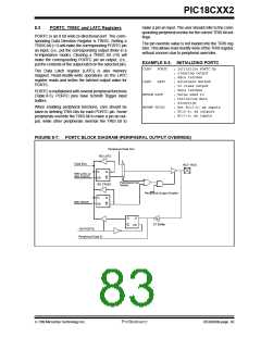
Each of the PORTB pins has a weak internal pull-up. A
single control bit can turn on all the pull-ups. This is per-
formed by clearing bit RBPU (INTCON2<7>). The
weak pull-up is automatically turned off when the port
pin is configured as an output. The pull-ups are dis-
abled on a Power-on Reset.
Note 1: I/O pins have diode protection to VDD and VSS.
2: To enable weak pull-ups, set the appropriate TRIS
bit(s) and clear the RBPU bit (INTCON2<7>).
FIGURE 8-5: BLOCK DIAGRAM OF
RB2:RB0 PINS
Four of PORTB’s pins, RB7:RB4, have an interrupt on
change feature. Only pins configured as inputs can
cause this interrupt to occur (i.e. any RB7:RB4 pin con-
figured as an output is excluded from the interrupt on
change comparison). The input pins (of RB7:RB4) are
compared with the old value latched on the last read of
PORTB. The “mismatch” outputs of RB7:RB4 are
OR’ed together to generate the RB Port Change Inter-
rupt with flag bit RBIF (INTCON<0>).
VDD
RBPU(2)
weak
P
pull-up
Data Latch
Data Bus
WR Port
D
Q
I/O
pin(1)
CK
TRIS Latch
D
Q
TTL
Input
Buffer
This interrupt can wake the device from SLEEP. The
user, in the interrupt service routine, can clear the inter-
rupt in the following manner:
WR TRIS
CK
a) Any read or write of PORTB (except with the
MOVFF instruction). This will end the mismatch
condition.
RD TRIS
RD Port
Q
D
b) Clear flag bit RBIF.
EN
A mismatch condition will continue to set flag bit RBIF.
Reading PORTB will end the mismatch condition and
allow flag bit RBIF to be cleared.
RB0/INT
Schmitt Trigger
Buffer
RD Port
The interrupt on change feature is recommended for
wake-up on key depression operation and operations
where PORTB is only used for the interrupt on change
feature. Polling of PORTB is not recommended while
using the interrupt on change feature.
Note 1: I/O pins have diode protection to VDD and VSS.
2: To enable weak pull-ups, set the appropriate TRIS
bit(s) and clear the RBPU bit (OPTION_REG<7>).
DS39026B-page 80
Preliminary
7/99 Microchip Technology Inc.

 MICROCHIP [ MICROCHIP ]