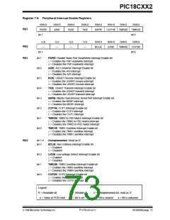
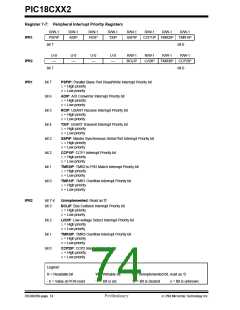
PIC18CXX2
The Data Latch register (LATA) is also memory
mapped. Read-modify-write operations on the LATA
register reads and writes the latched output value for
PORTA.
8.0
I/O PORTS
Depending on the device selected, there are either five
ports or three ports available. Some pins of the I/O
ports are multiplexed with an alternate function from
the peripheral features on the device. In general, when
a peripheral is enabled, that pin may not be used as a
general purpose I/O pin.
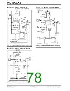
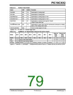
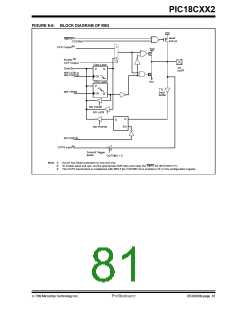
The RA4 pin is multiplexed with the Timer0 module
clock input to become the RA4/T0CKI pin. The RA4/
T0CKI pin is a Schmitt Trigger input and an open drain
output. All other RA port pins have TTL input levels and
full CMOS output drivers.
Each port has three registers for its operation. These
registers are:
The other PORTA pins are multiplexed with analog
inputs and the analog VREF+ and VREF- inputs. The
operation of each pin is selected by clearing/setting the
control bits in the ADCON1 register (A/D Control
Register1).
• TRIS register (Data Direction register)
• PORT register (reads the levels on the pins of the
device)
• LAT register (output latch)
The data latch (LAT register) is useful for read-modify-
write operations on the value that the I/O pins are driv-
ing.
Note: On a Power-on Reset, these pins are con-
figured as analog inputs and read as '0'.
The TRISA register controls the direction of the RA
pins, even when they are being used as analog inputs.
The user must ensure the bits in the TRISA register are
maintained set when using them as analog inputs.
8.1
PORTA, TRISA and LATA Registers
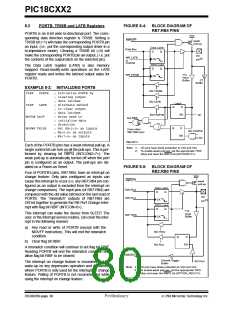
PORTA is a 6-bit wide bi-directional port. The corre-
sponding data direction register is TRISA. Setting a
TRISA bit (=1) will make the corresponding PORTA pin
an input, (i.e., put the corresponding output driver in a
hi-impedance mode). Clearing a TRISA bit (=0) will
make the corresponding PORTA pin an output, (i.e., put
the contents of the output latch on the selected pin).
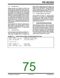
EXAMPLE 8-1: INITIALIZING PORTA
CLRF PORTA
; Initialize PORTA by
; clearing output
; data latches
CLRF LATA
; Alternate method
; to clear output
; data latches
Note: On a Power-on Reset, these pins are con-
figured as inputs and read as '0'.
MOVLW 0x07
MOVWF ADCON1
MOVLW 0xCF
; Configure A/D
; for digital inputs
; Value used to
Reading the PORTA register reads the status of the
pins, whereas writing to it will write to the port latch.
; initialize data
; direction
MOVWF TRISA
; Set RA<3:0> as inputs
; RA<5:4> as outputs
7/99 Microchip Technology Inc.
Preliminary
DS39026B-page 77

 MICROCHIP [ MICROCHIP ]