PIC18CXX2
8.4
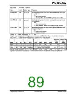
PORTD, TRISD and LATD Registers
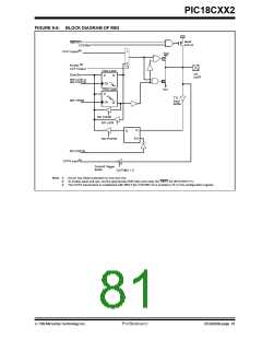
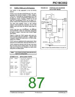
FIGURE 8-8: PORTD BLOCK DIAGRAM
IN I/O PORT MODE
This section is applicable to only the PIC18C4X2
devices.
PORTD is an 8 bit wide bi-directional port. The corre-
sponding Data Direction Register is TRISD. Setting a
TRISD bit (=1) will make the corresponding PORTD pin
an input, (i.e., put the corresponding output driver in a
hi-impedance mode). Clearing a TRISD bit (=0) will
make the corresponding PORTD pin an output, (i.e.,
put the contents of the output latch on the selected pin).
RD LATD
Data
Bus
D
Q
I/O pin(1)
WR LATD
or
PORTD
CK
Data Latch
D
Q
The Data Latch Register (LATD) is also memory
mapped. Read-modify-write operations on the LATD
register reads and writes the latched output value for
PORTD.
WR TRISD
Schmitt
Trigger
input
CK
TRIS Latch
buffer
PORTD is an 8-bit port with Schmitt Trigger input buff-
ers. Each pin is individually configurable as an input or
output.
RD TRISD
PORTD can be configured as an 8-bit wide micropro-
cessor port (parallel slave port) by setting control bit
PSPMODE (TRISE<4>). In this mode, the input buffers
are TTL. See Section 8.6 for additional information on
the Parallel Slave Port (PSP).
Q
D
EN
EN
RD PORTD
EXAMPLE 8-4: INITIALIZING PORTD
Note 1: I/O pins have protection diodes to VDD and VSS.
CLRF
PORTD ; Initialize PORTD by
; clearing output
; data latches
CLRF
LATD
; Alternate method
; to clear output
; data latches
MOVLW 0xCF
; Value used to
; initialize data
; direction
MOVWF TRISD
; Set RD<3:0> as inputs
; RD<5:4> as outputs
; RD<7:6> as inputs
7/99 Microchip Technology Inc.
Preliminary
DS39026B-page 85

 MICROCHIP [ MICROCHIP ]