PIC18CXX2
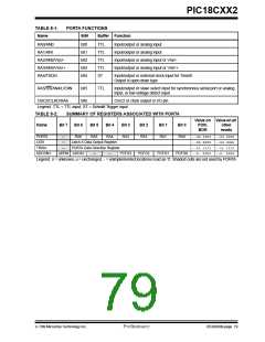
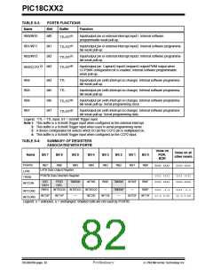
TABLE 8-1:
Name
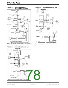
PORTA FUNCTIONS
Bit#
Buffer Function
RA0/AN0
bit0
bit1
bit2
bit3
bit4
TTL
TTL
TTL
TTL
ST
Input/output or analog input
RA1/AN1
Input/output or analog input
RA2/AN2/VREF-
RA3/AN3/VREF+
RA4/T0CKI
Input/output or analog input or VREF-
Input/output or analog input or VREF+
Input/output or external clock input for Timer0
Output is open drain type
RA5/SS/AN4/LVDIN
OSC2/CLKO/RA6
bit5
bit6
TTL
Input/output or slave select input for synchronous serial port or analog
input, or low voltage detect input
OSC2 or clock output or I/O pin
Legend: TTL = TTL input, ST = Schmitt Trigger input
TABLE 8-2:
SUMMARY OF REGISTERS ASSOCIATED WITH PORTA
Value on Valueon all
Name
Bit 7
Bit 6
Bit 5
Bit 4
Bit 3
Bit 2
Bit 1
Bit 0
POR,
BOR
other
resets
PORTA
LATA
—
—
—
RA6
RA5
RA4
RA3
RA2
RA1
RA0
--0x 0000 --0u 0000
--xx xxxx --uu uuuu
--11 1111 --11 1111
Latch A Data Output Register
PORTA Data Direction Register
TRISA
ADCON1
ADFM ADCS2
—
—
PCFG3
PCFG2
PCFG1
PCFG0 --0- 0000 --0- 0000
Legend: x = unknown, u = unchanged, - = unimplemented locations read as ’0’. Shaded cells are not used by PORTA.
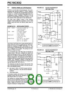
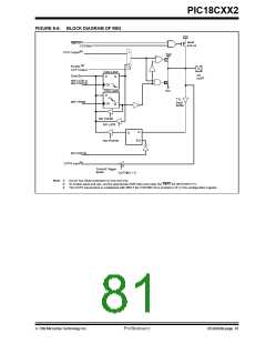
7/99 Microchip Technology Inc.
Preliminary
DS39026B-page 79

 MICROCHIP [ MICROCHIP ]