PIC18CXX2
The operation of CCP1 is identical to that of CCP2, with
the exception of the special event trigger. Therefore,
operation of a CCP module in the following sections is
described with respect to CCP1.
13.0 CAPTURE/COMPARE/PWM
(CCP) MODULES
Each CCP (Capture/Compare/PWM) module contains
a 16-bit register which can operate as a 16-bit capture
register, as a 16-bit compare register or as a PWM
master/slave Duty Cycle register. Table 13-1 shows the
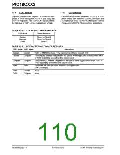
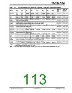
timer resources of the CCP module modes.
Table 13-2 shows the interaction of the CCP modules.
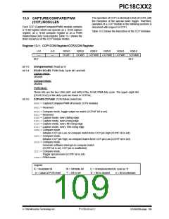
Register 13-1: CCP1CON Register/CCP2CON Register
U-0
U-0
R/W-0
R/W-0
R/W-0
R/W-0
R/W-0
R/W-0
—
—
DCxB1
DCxB0
CCPxM3 CCPxM2 CCPxM1 CCPxM0
bit 0
bit 7
bit 7:6
bit 5:4
Unimplemented: Read as '0'
DCxB1:DCxB0: PWM Duty Cycle bit1 and bit0
Capture Mode:
Unused
Compare Mode:
Unused
PWM Mode:
These bits are the two LSbs (bit1 and bit0) of the 10-bit PWM duty cycle. The upper eight bits
(DCx9:DCx2) of the duty cycle are found in CCPRxL.
bit 3:0
CCPxM3:CCPxM0: CCPx Mode Select bits
0000= Capture/Compare/PWM off (resets CCPx module)
0001= Reserved
0010= Compare mode, toggle output on match (CCPxIF bit is set)
0011= Reserved
0100= Capture mode, every falling edge
0101= Capture mode, every rising edge
0110= Capture mode, every 4th rising edge
0111= Capture mode, every 16th rising edge
1000= Compare mode,
Initialize CCP pin Low, on compare match force CCP pin High (CCPIF bit is set)
1001= Compare mode,
Initialize CCP pin High, on compare match force CCP pin Low (CCPIF bit is set)
1010= Compare mode,
Generate software interrupt on compare match
(CCPIF bit is set, CCP pin is unaffected)
1011= Compare mode,
Trigger special event (CCPIF bit is set)
11xx= PWM mode
Legend:
R = Readable bit
W = Writable bit
’1’ = Bit is set
U = Unimplemented bit, read as ‘0’
’0’ = Bit is cleared x = Bit is unknown
- n = Value at POR reset
7/99 Microchip Technology Inc.
Preliminary
DS39026B-page 109

 MICROCHIP [ MICROCHIP ]