PIC18CXX2
12.2
Timer1 Oscillator
12.4
Resetting Timer3 Using a CCP Trigger
Output
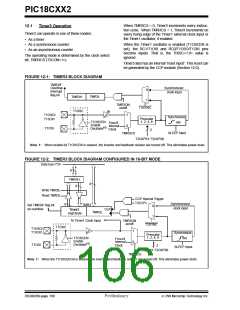
The Timer1 oscillator may be used as the clock source
for Timer3. The Timer1 oscillator is enabled by setting
the T1OSCEN (T1CON<3>) bit. The oscillator is a low
power oscillator rated up to 200 KHz. See Section 10.0
for further details.
If the CCP module is configured in compare mode to
generate a “special event trigger" (CCP1M3:CCP1M0
= 1011), this signal will reset Timer3.
Note: The special event triggers from the CCP
module will not set interrupt flag bit
TMR3IF (PIR1<0>).
12.3
Timer3 Interrupt
The TMR3 Register pair (TMR3H:TMR3L) increments
from 0000h to FFFFh and rolls over to 0000h. The
TMR3 Interrupt, if enabled, is generated on overflow
which is latched in interrupt flag bit TMR3IF (PIR2<1>).
This interrupt can be enabled/disabled by setting/clear-
ing TMR3 interrupt enable bit TMR3IE (PIE2<1>).
Timer3 must be configured for either timer or synchro-
nized counter mode to take advantage of this feature. If
Timer3 is running in asynchronous counter mode, this
reset operation may not work. In the event that a write
to Timer3 coincides with a special event trigger from
CCP1, the write will take precedence. In this mode of
operation, the CCPR1H:CCPR1L registers pair effec-
tively becomes the period register for Timer3.
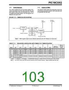
TABLE 12-1: REGISTERS ASSOCIATED WITH TIMER3 AS A TIMER/COUNTER
Value on
POR,
BOR
Value on
all other
resets
Name
Bit 7
Bit 6
Bit 5
Bit 4
Bit 3
Bit 2
Bit 1
Bit 0
INTCON
GIE/
GIEH
PEIE/
GIEL
TMR0IE
INT0IE
RBIE
TMR0IF
INT0IF
RBIF
0000 000x 0000 000u
PIR2
—
—
—
—
—
—
—
—
—
—
—
—
BCLIF
BCLIE
BCLIP
LVDIF
LVDIE
LVDIP
TMR3IF
TMR3IE
TMR3IP
CCP2IF
CCP2IE
CCP2IP
0000 0000 0000 0000
0000 0000 0000 0000
0000 0000 0000 0000
xxxx xxxx uuuu uuuu
xxxx xxxx uuuu uuuu
PIE2
IPR2
TMR3L
TMR3H
T1CON
T3CON
Holding register for the Least Significant Byte of the 16-bit TMR3 register
Holding register for the Most Significant Byte of the 16-bit TMR3 register
—
—
—
T1CKPS1 T1CKPS0 T1OSCEN T1SYNC TMR1CS TMR1ON --00 0000 --uu uuuu
T3CKPS2 T3CKPS1 T3CKPS0 T3CCP1 T3SYNC TMR3CS TMR3ON -000 0000 -uuu uuuu
Legend: x = unknown, u = unchanged, - = unimplemented read as ’0’. Shaded cells are not used by the Timer1 module.
7/99 Microchip Technology Inc.
Preliminary
DS39026B-page 107

 MICROCHIP [ MICROCHIP ]