PIC18CXX2
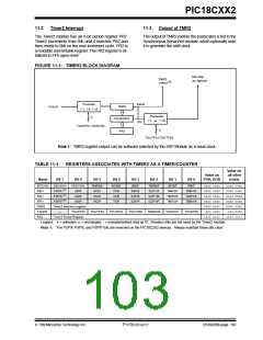
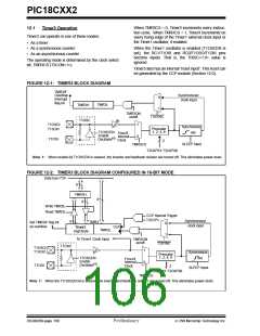
Figure 12-1 is a simplified block diagram of the Timer3
module.
12.0 TIMER3 MODULE
The Timer3 module timer/counter has the following fea-
tures:
Register 12-1 shows the Timer3 control register. This
register controls the operating mode of the Timer3
module and sets the CCP clock source.
• 16-bit timer/counter
(Two 8-bit registers; TMR3H and TMR3L)
Register 10-1 shows the Timer1 control register. This
register controls the operating mode of the Timer1
module, as well as contains the Timer1 oscillator
enable bit (T1OSCEN), which can be a clock source for
Timer3.
• Readable and writable (both registers)
• Internal or external clock select
• Interrupt on overflow from FFFFh to 0000h
• Reset from CCP module trigger
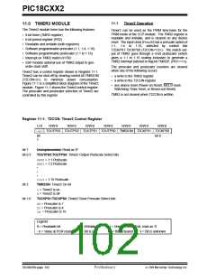
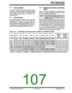
Register 12-1: T3CON: Timer3 Control Register
R/W-0
RD16
R/W-0
R/W-0
R/W-0
R/W-0
R/W-0
R/W-0
R/W-0
T3CCP2 T3CKPS1 T3CKPS0
T3CCP1
T3SYNC TMR3CS TMR3ON
bit 0
bit 7
bit 7
RD16: 16-bit Read/Write Mode Enable
1= Enables register Read/Write of Timer3 in one 16-bit operation
0= Enables register Read/Write of Timer3 in two 8-bit operations
bit 6,3
T3CCP2:T3CCP1: Timer3 and Timer1 to CCPx Enable bits
1x= Timer3 is the clock source for compare/capture CCP modules
01= Timer3 is the clock source for compare/capture of CCP2,
Timer1 is the clock source for compare/capture of CCP1
00= Timer1 is the clock source for compare/capture CCP modules
bit 5:4
bit 2
T3CKPS1:T3CKPS0: Timer3 Input Clock Prescale Select bits
11= 1:8 Prescale value
10= 1:4 Prescale value
01= 1:2 Prescale value
00= 1:1 Prescale value
T3SYNC: Timer3 External Clock Input Synchronization Control bit
(Not usable if the system clock comes from Timer1/Timer3)
When TMR3CS = 1:
1= Do not synchronize external clock input
0= Synchronize external clock input
When TMR3CS = 0:
This bit is ignored. Timer3 uses the internal clock when TMR3CS = 0.
bit 1
bit 0
TMR3CS: Timer3 Clock Source Select bit
1= External clock input from Timer1 oscillator or T1CKI (on the rising edge after the first falling
edge)
0= Internal clock (Fosc/4)
TMR3ON: Timer3 On bit
1= Enables Timer3
0= Stops Timer3
Legend:
R = Readable bit
W = Writable bit
’1’ = Bit is set
U = Unimplemented bit, read as ‘0’
’0’ = Bit is cleared x = Bit is unknown
- n = Value at POR reset
7/99 Microchip Technology Inc.
Preliminary
DS39026B-page 105

 MICROCHIP [ MICROCHIP ]