PIC18CXX2
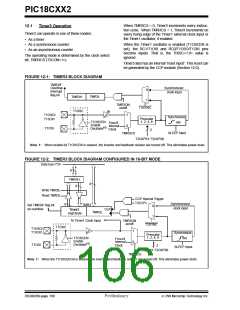
When TMR3CS = 0, Timer3 increments every instruc-
tion cycle. When TMR3CS = 1, Timer3 increments on
every rising edge of the Timer1 external clock input or
the Timer1 oscillator, if enabled.
12.1
Timer3 Operation
Timer3 can operate in one of these modes:
• As a timer
• As a synchronous counter
• As an asynchronous counter
When the Timer1 oscillator is enabled (T1OSCEN is
set), the RC1/T1OSI and RC0/T1OSO/T1CKI pins
become inputs. That is, the TRISC<1:0> value is
ignored.
The operating mode is determined by the clock select
bit, TMR3CS (T3CON<1>).
Timer3 also has an internal “reset input”. This reset can
be generated by the CCP module (Section 12.0).
FIGURE 12-1: TIMER3 BLOCK DIAGRAM
TMR3IF
Overflow
Interrupt
Synchronized
0
clock input
flag bit
TMR3L
TMR3H
T1OSC
1
TMR3ON
on/off
T3SYNC
(3)
T1OSO/
T13CKI
1
Synchronize
det
Prescaler
1, 2, 4, 8
T1OSCEN
Enable
Oscillator
Fosc/4
Internal
Clock
0
(1)
T1OSI
2
SLEEP input
TMR3CS
T3CKPS1:T3CKPS0
Note 1: When enable bit T1OSCEN is cleared, the inverter and feedback resistor are turned off. This eliminates power drain.
FIGURE 12-2: TIMER3 BLOCK DIAGRAM CONFIGURED IN 16-BIT MODE
Data bus<7:0>
8
TMR3H
8
8
Write TMR3L
Read TMR3L
CCP Special Trigger
T3CCPx
Synchronized
clock input
8
TMR3
Set TMR3IF flag bit
on overflow
0
CLR
Timer3
High Byte
TMR3L
1
To Timer1 Clock Input
TMR3ON
on/off
T3SYNC
T1OSC
T1OSO/
T13CKI
1
Synchronize
det
Prescaler
1, 2, 4, 8
T1OSCEN
Enable
Oscillator
FOSC/4
Internal
Clock
0
(1)
T1OSI
2
SLEEP input
T3CKPS1:T3CKPS0
TMR3CS
Note 1: When the T1OSCEN bit is cleared, the inverter and feedback resistor are turned off. This eliminates power drain.
DS39026B-page 106
Preliminary
7/99 Microchip Technology Inc.

 MICROCHIP [ MICROCHIP ]