PIC18CXX2
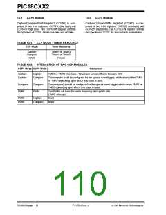
13.4.2 TIMER1/TIMER3 MODE SELECTION
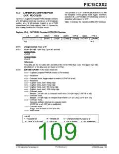
13.4
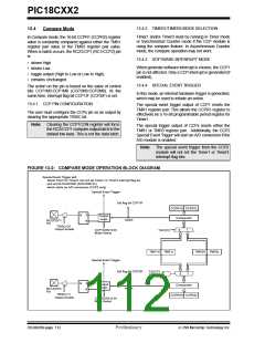
Compare Mode
Timer1 and/or Timer3 must be running in Timer mode
or Synchronized Counter mode if the CCP module is
using the compare feature. In Asynchronous Counter
mode, the compare operation may not work.
In Compare mode, the 16-bit CCPR1 (CCPR2) register
value is constantly compared against either the TMR1
register pair value or the TMR3 register pair value.
When a match occurs, the RC2/CCP1 (RC1/CCP2) pin
is:
13.4.3 SOFTWARE INTERRUPT MODE
• driven High
When generate software interrupt is chosen, the CCP1
pin is not affected. Only a CCP interrupt is generated (if
enabled).
• driven Low
• toggle output (High to Low or Low to High)
• remains Unchanged
13.4.4 SPECIAL EVENT TRIGGER
The action on the pin is based on the value of control
bits CCP1M3:CCP1M0 (CCP2M3:CCP2M0). At the
same time, interrupt flag bit CCP1IF (CCP2IF) is set.
In this mode, an internal hardware trigger is generated,
which may be used to initiate an action.
13.4.1 CCP PIN CONFIGURATION
The special event trigger output of CCP1 resets the
TMR1 register pair. This allows the CCPR1 register to
effectively be a 16-bit programmable period register for
Timer1.
The user must configure the CCPx pin as an output by
clearing the appropriate TRISC bit.
Note: Clearing the CCP1CON register will force
the RC2/CCP1 compare output latch to the
default low level. This is not the data latch.
The special trigger output of CCPx resets either the
TMR1 or TMR3 register pair. Additionally, the CCP2
Special Event Trigger will start an A/D conversion if the
A/D module is enabled.
Note: The special event trigger from the CCP2
module will not set the Timer1 or Timer3
interrupt flag bits.
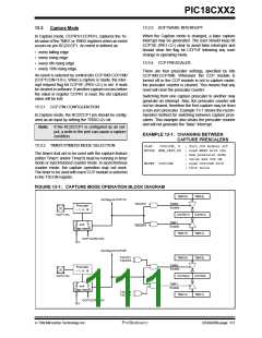
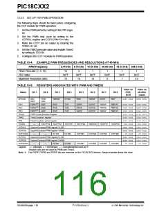
FIGURE 13-2: COMPARE MODE OPERATION BLOCK DIAGRAM
Special Event Trigger will:
Reset Timer1or Timer3, but not set Timer1 or Timer3 interrupt flag bit,
and set bit GO/DONE (ADCON0<2>)
which starts an A/D conversion (CCP2 only)
Special Event Trigger
Set flag bit CCP1IF
CCPR1H CCPR1L
Comparator
Q
S
R
Output
Logic
match
RC2/CCP1
Pin
TRISC<2>
Output Enable
1
0
CCP1CON<3:0>
Mode Select
T3CCP2
TMR1H TMR1L
TMR3H TMR3L
Special Event Trigger
Set flag bit CCP2IF
match
T3CCP1
T3CCP2
0
1
Q
S
R
Output
Logic
Comparator
RC1/CCP2
Pin
TRISC<1>
Output Enable
CCPR2H CCPR2L
CCP2CON<3:0>
Mode Select
DS39026B-page 112
Preliminary
7/99 Microchip Technology Inc.

 MICROCHIP [ MICROCHIP ]