PIC18CXX2
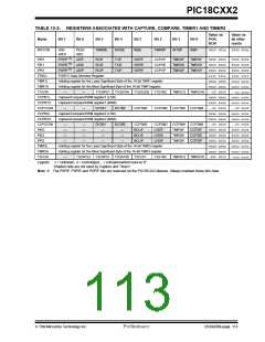
TABLE 13-3: REGISTERS ASSOCIATED WITH CAPTURE, COMPARE, TIMER1 AND TIMER3
Value on
POR,
BOR
Value on
all other
resets
Name
Bit 7
Bit 6
Bit 5
Bit 4
Bit 3
Bit 2
Bit 1
Bit 0
INTCON
GIE/
GIEH
PEIE/
GIEL
TMR0IE
INT0IE
RBIE
TMR0IF
INT0IF
RBIF
0000 000x
0000 000u
(1)
(1)
(1)
PIR1
PSPIF
PSPIE
PSPIP
ADIF
ADIE
ADIP
RCIF
RCIE
RCIP
TXIF
TXIE
TXIP
SSPIF
SSPIE
SSPIP
CCP1IF
CCP1IE
CCP1IP
TMR2IF
TMR2IE
TMR2IP
TMR1IF
TMR1IE
TMR1IP
0000 0000
0000 0000
0000 0000
1111 1111
xxxx xxxx
xxxx xxxx
0000 0000
0000 0000
0000 0000
1111 1111
uuuu uuuu
uuuu uuuu
--uu uuuu
uuuu uuuu
uuuu uuuu
--00 0000
uuuu uuuu
uuuu uuuu
--00 0000
0000 0000
0000 0000
0000 0000
uuuu uuuu
uuuu uuuu
-uuu uuuu
PIE1
IPR1
TRISC
TMR1L
TMR1H
T1CON
CCPR1L
CCPR1H
CCP1CON
CCPR2L
CCPR2H
CCP2CON
PIR2
PORTC Data Direction Register
Holding register for the Least Significant Byte of the 16-bit TMR1 register
Holding register for the Most Significant Byte of the 16-bit TMR1register
—
—
T1CKPS1 T1CKPS0
T1OSCEN
T1SYNC
TMR1CS TMR1ON --00 0000
xxxx xxxx
Capture/Compare/PWM register1 (LSB)
Capture/Compare/PWM register1 (MSB)
xxxx xxxx
—
—
DC1B1
DC1B0
CCP1M3
CCP1M2
CCP1M1 CCP1M0
--00 0000
xxxx xxxx
xxxx xxxx
--00 0000
0000 0000
0000 0000
0000 0000
xxxx xxxx
xxxx xxxx
Capture/Compare/PWM register2 (LSB)
Capture/Compare/PWM register2 (MSB)
—
—
—
—
—
—
—
—
DC2B1
—
DC2B0
—
CCP2M3
BCLIF
CCP2M2
LVDIF
CCP2M1 CCP2M0
TMR3IF
TMR3IE
TMR3IP
CCP2IF
CCP2IE
CCP2IP
PIE2
—
—
BCLIE
BCLIP
LVDIE
IPR2
—
—
LVDIP
TMR3L
TMR3H
T3CON
Holding register for the Least Significant Byte of the 16-bit TMR3 register
Holding register for the Most Significant Byte of the 16-bit TMR3 register
—
T3CKPS2
T3CKPS1 T3CKPS0
T3CCP1
T3SYNC
TMR3CS TMR3ON -000 0000
Legend: x = unknown, u = unchanged, - = unimplemented read as ’0’.
Shaded cells are not used by Capture and Timer1.
Note 1: The PSPIF, PSPIE and PSPIP bits are reserved on the PIC18C2x2 devices. Always maintain these bits clear.
7/99 Microchip Technology Inc.
Preliminary
DS39026B-page 113

 MICROCHIP [ MICROCHIP ]