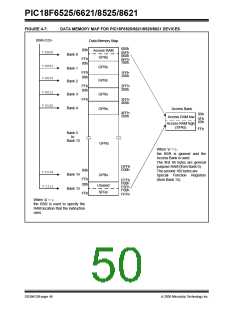
PIC18F6525/6621/8525/8621
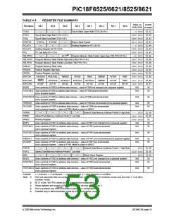
TABLE 4-3:
File Name
TOSU
REGISTER FILE SUMMARY
Value on
POR, BOR on page:
Details
Bit 7
Bit 6
Bit 5
Bit 4
Bit 3
Bit 2
Bit 1
Bit 0
—
—
—
Top-of-Stack Upper Byte (TOS<20:16>)
---0 0000 32, 42
0000 0000 32, 42
0000 0000 32, 42
00-0 0000 32, 43
---0 0000 32, 44
0000 0000 32, 44
0000 0000 32, 44
--00 0000 32, 69
0000 0000 32, 69
0000 0000 32, 69
0000 0000 32, 69
xxxx xxxx 32, 85
xxxx xxxx 32, 85
0000 000x 32, 89
1111 1111 32, 90
1100 0000 32, 91
TOSH
Top-of-Stack High Byte (TOS<15:8>)
Top-of-Stack Low Byte (TOS<7:0>)
TOSL
STKPTR
PCLATU
PCLATH
PCL
STKFUL
—
STKUNF
—
—
—
Return Stack Pointer
Holding Register for PC<20:16>
Holding Register for PC<15:8>
PC Low Byte (PC<7:0>)
(2)
TBLPTRU
—
—
bit 21
Program Memory Table Pointer Upper Byte (TBLPTR<20:16>)
TBLPTRH Program Memory Table Pointer High Byte (TBLPTR<15:8>)
TBLPTRL
TABLAT
PRODH
PRODL
Program Memory Table Pointer Low Byte (TBLPTR<7:0>)
Program Memory Table Latch
Product Register High Byte
Product Register Low Byte
INTCON
INTCON2
INTCON3
INDF0
GIE/GIEH PEIE/GIEL
TMR0IE
INTEDG1
INT3IE
INT0IE
INTEDG2
INT2IE
RBIE
INTEDG3
INT1IE
TMR0IF
TMR0IP
INT3IF
INT0IF
INT3IP
INT2IF
RBIF
RBIP
RBPU
INTEDG0
INT1IP
INT2IP
INT1IF
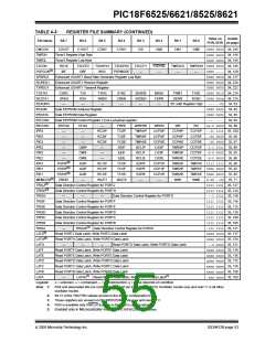
Uses contents of FSR0 to address data memory – value of FSR0 not changed (not a physical register)
N/A
N/A
56
56
POSTINC0 Uses contents of FSR0 to address data memory – value of FSR0 post-incremented
(not a physical register)
POSTDEC0 Uses contents of FSR0 to address data memory – value of FSR0 post-decremented
(not a physical register)
N/A
56
PREINC0
PLUSW0
Uses contents of FSR0 to address data memory – value of FSR0 pre-incremented (not a physical register)
N/A
N/A
56
56
Uses contents of FSR0 to address data memory – value of FSR0 pre-incremented
(not a physical register) – value of FSR0 offset by value in WREG
FSR0H
FSR0L
WREG
INDF1
—
—
—
—
Indirect Data Memory Address Pointer 0 High Byte ---- 0000 32, 56
xxxx xxxx 32, 56
Indirect Data Memory Address Pointer 0 Low Byte
Working Register
xxxx xxxx
N/A
32
56
56
Uses contents of FSR1 to address data memory – value of FSR1 not changed (not a physical register)
POSTINC1 Uses contents of FSR1 to address data memory – value of FSR1 post-incremented
(not a physical register)
N/A
POSTDEC1 Uses contents of FSR1 to address data memory – value of FSR1 post-decremented
(not a physical register)
N/A
56
PREINC1
PLUSW1
Uses contents of FSR1 to address data memory – value of FSR1 pre-incremented (not a physical register)
N/A
N/A
56
56
Uses contents of FSR1 to address data memory – value of FSR1 pre-incremented
(not a physical register) – value of FSR1 offset by value in WREG
FSR1H
FSR1L
BSR
—
—
—
—
Indirect Data Memory Address Pointer 1 High Byte ---- 0000 32, 56
xxxx xxxx 33, 56
Indirect Data Memory Address Pointer 1 Low Byte
—
—
—
—
Bank Select Register
---- 0000 33, 55
INDF2
Uses contents of FSR2 to address data memory – value of FSR2 not changed (not a physical register)
N/A
N/A
56
56
POSTINC2 Uses contents of FSR2 to address data memory – value of FSR2 post-incremented
(not a physical register)
POSTDEC2 Uses contents of FSR2 to address data memory – value of FSR2 post-decremented
(not a physical register)
N/A
56
Legend:
Note 1:
x= unknown, u= unchanged, – = unimplemented, q= value depends on condition
RA6 and associated bits are configured as a port pin in RCIO and ECIO Oscillator modes only and read ‘0’ in all other
oscillator modes.
2:
3:
4:
Bit 21 of the TBLPTRU allows access to the device configuration bits.
These registers are unused on PIC18F6525/6621 devices and read as ‘0’.
RG5 is available only if MCLR function is disabled in configuration.
5: Enabled only in Microcontroller mode for PIC18F8525/8621 devices.
2005 Microchip Technology Inc.
DS39612B-page 51

 MICROCHIP [ MICROCHIP ]