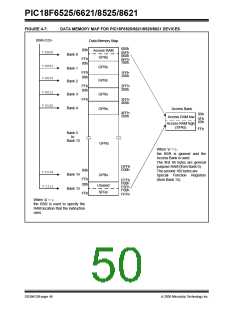
PIC18F6525/6621/8525/8621
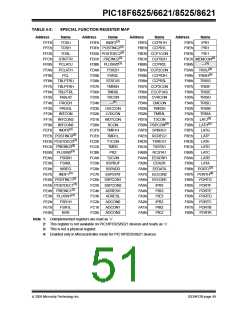
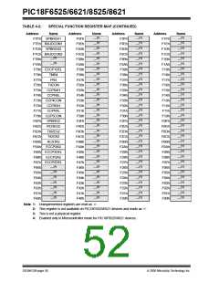
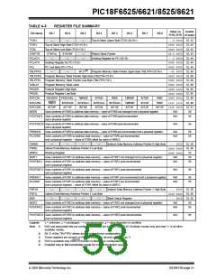
TABLE 4-3:
REGISTER FILE SUMMARY (CONTINUED)
Value on
POR, BOR on page:
Details
File Name
Bit 7
Bit 6
Bit 5
Bit 4
Bit 3
Bit 2
Bit 1
Bit 0
PREINC2
PLUSW2
Uses contents of FSR2 to address data memory – value of FSR2 pre-incremented
(not a physical register)
N/A
N/A
56
56
Uses contents of FSR2 to address data memory – value of FSR2 pre-incremented
(not a physical register) – value of FSR2 offset by value in WREG
FSR2H
—
—
—
—
Indirect Data Memory Address Pointer 2 High Byte ---- 0000 33, 56
xxxx xxxx 33, 56
FSR2L
Indirect Data Memory Address Pointer 2 Low Byte
STATUS
TMR0H
TMR0L
—
—
—
N
OV
Z
DC
C
---x xxxx 33, 58
0000 0000 33, 133
xxxx xxxx 33, 133
1111 1111 33, 131
---- 0000 25, 33
--00 0101 33, 255
Timer0 Register High Byte
Timer0 Register Low Byte
T0CON
OSCCON
LVDCON
WDTCON
RCON
TMR0ON
T08BIT
—
T0CS
—
T0SE
—
PSA
LOCK
LVDL3
—
T0PS2
PLLEN
LVDL2
—
T0PS1
SCS1
LVDL1
—
T0PS0
SCS0
LVDL0
—
—
—
IRVST
—
LVDEN
—
—
—
SWDTEN ---- ---0 33, 267
IPEN
—
—
RI
TO
PD
POR
BOR
0--1 11qq 33, 59,
101
TMR1H
Timer1 Register High Byte
Timer1 Register Low Byte
xxxx xxxx 33, 139
xxxx xxxx 33, 139
TMR1L
T1CON
RD16
—
T1CKPS1
T1CKPS0 T1OSCEN T1SYNC
TMR1CS
TMR1ON 0-00 0000 33, 139
0000 0000 33, 142
TMR2
Timer2 Register
PR2
Timer2 Period Register
1111 1111 33, 142
T2CON
—
T2OUTPS3 T2OUTPS2 T2OUTPS1 T2OUTPS0 TMR2ON T2CKPS1 T2CKPS0 -000 0000 33, 142
SSPBUF
SSPADD
SSPSTAT
SSPCON1
SSPCON2
ADRESH
ADRESL
ADCON0
ADCON1
ADCON2
CCPR1H
CCPR1L
CCP1CON
CCPR2H
CCPR2L
CCP2CON
CCPR3H
CCPR3L
CCP3CON
MSSP Receive Buffer/Transmit Register
2
xxxx xxxx 33, 181
0000 0000 33, 181
0000 0000 33, 174
2
MSSP Address Register in I C Slave mode. MSSP Baud Rate Reload Register in I C Master mode.
SMP
WCOL
GCEN
CKE
D/A
P
S
R/W
SSPM2
PEN
UA
BF
SSPOV
ACKSTAT
SSPEN
ACKDT
CKP
SSPM3
RCEN
SSPM1
RSEN
SSPM0 0000 0000 33, 175
ACKEN
SEN
0000 0000 33, 185
xxxx xxxx 33, 241
xxxx xxxx 33, 241
--00 0000 34, 233
--00 0000 34, 234
0-00 0000 34, 235
xxxx xxxx 34, 172
xxxx xxxx 34, 172
A/D Result Register High Byte
A/D Result Register Low Byte
—
—
—
—
—
CHS3
VCFG1
ACQT2
CHS2
VCFG0
ACQT1
CHS1
PCFG3
ACQT0
CHS0
PCFG2
ADCS2
GO/DONE
PCFG1
ADON
PCFG0
ADCS0
ADFM
ADCS1
Enhanced Capture/Compare/PWM Register 1 High Byte
Enhanced Capture/Compare/PWM Register 1 Low Byte
P1M1
P1M0
DC1B1
DC1B0
CCP1M3
CCP2M3
CCP3M3
CCP1M2
CCP2M2
CCP3M2
CCP1M1
CCP2M1
CCP3M1
CCP1M0 0000 0000 34, 157
xxxx xxxx 34, 172
Enhanced Capture/Compare/PWM Register 2 High Byte
Enhanced Capture/Compare/PWM Register 2 Low Byte
xxxx xxxx 34, 172
P2M1
P2M0
DC2B1
DC2B0
CCP2M0 0000 0000 34, 157
xxxx xxxx 34, 172
Enhanced Capture/Compare/PWM Register 3 High Byte
Enhanced Capture/Compare/PWM Register 3 Low Byte
xxxx xxxx 34, 172
P3M1
P3M0
DC3B1
DC2B0
CCP3M0 0000 0000 34, 157
ECCP1AS ECCP1ASE ECCP1AS2 ECCP1AS1 ECCP1AS0 PSS1AC1 PSS1AC0 PSS1BD1 PSS1BD0 0000 0000 34, 169
CVRCON
CVREN
CVROE
CVRR
CVRSS
CVR3
CVR2
CVR1
CVR0
0000 0000 34, 249
Legend:
Note 1:
x= unknown, u= unchanged, – = unimplemented, q= value depends on condition
RA6 and associated bits are configured as a port pin in RCIO and ECIO Oscillator modes only and read ‘0’ in all other
oscillator modes.
2:
3:
4:
Bit 21 of the TBLPTRU allows access to the device configuration bits.
These registers are unused on PIC18F6525/6621 devices and read as ‘0’.
RG5 is available only if MCLR function is disabled in configuration.
5: Enabled only in Microcontroller mode for PIC18F8525/8621 devices.
DS39612B-page 52
2005 Microchip Technology Inc.

 MICROCHIP [ MICROCHIP ]