PIC18F6525/6621/8525/8621
4.10
Access Bank
4.11 Bank Select Register (BSR)
The Access Bank is an architectural enhancement,
which is very useful for C compiler code optimization.
The techniques used by the C compiler may also be
useful for programs written in assembly.
The need for a large general purpose memory space
dictates a RAM banking scheme. The data memory is
partitioned into sixteen banks. When using direct
addressing, the BSR should be configured for the
desired bank.
This data memory region can be used for:
BSR<3:0> holds the upper 4 bits of the 12-bit RAM
address. The BSR<7:4> bits will always read ‘0’s and
writes will have no effect.
• Intermediate computational values
• Local variables of subroutines
• Faster context saving/switching of variables
• Common variables
A
MOVLB instruction has been provided in the
instruction set to assist in selecting banks.
• Faster evaluation/control of SFRs (no banking)
If the currently selected bank is not implemented, any
read will return all ‘0’s and all writes are ignored. The
STATUS register bits will be set/cleared as appropriate
for the instruction performed.
The Access Bank is comprised of the upper 160 bytes
in Bank 15 (SFRs) and the lower 96 bytes in Bank 0.
These two sections will be referred to as Access RAM
High and Access RAM Low, respectively. Figure 4-7
indicates the Access RAM areas.
Each Bank extends up to FFh (256 bytes). All data
memory is implemented as static RAM.
A bit in the instruction word specifies if the operation is
to occur in the bank specified by the BSR register or in
the Access Bank. This bit is denoted by the ‘a’ bit (for
access bit).
A MOVFFinstruction ignores the BSR since the 12-bit
addresses are embedded into the instruction word.
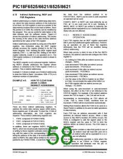
Section 4.12 “Indirect Addressing, INDF and FSR
Registers” provides a description of indirect address-
ing which allows linear addressing of the entire RAM
space.
When forced in the Access Bank (a = 0), the last
address in Access RAM Low is followed by the first
address in Access RAM High. Access RAM High maps
the Special Function Registers so that these registers
can be accessed without any software overhead. This is
useful for testing status flags and modifying control bits.
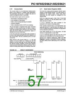
FIGURE 4-8:
DIRECT ADDRESSING
Direct Addressing
(3)
From Opcode
BSR<3:0>
7
0
(2)
(3)
Bank Select
Location Select
00h
01h
100h
0Eh
E00h
0Fh
F00h
000h
Data
Memory(1)
0FFh
1FFh
EFFh
FFFh
Bank 0
Bank 1
Bank 14 Bank 15
Note 1: For register file map detail, see Table 4-2.
2: The access bit of the instruction can be used to force an override of the selected bank (BSR<3:0>) to the
registers of the Access Bank.
3: The MOVFFinstruction embeds the entire 12-bit address in the instruction.
2005 Microchip Technology Inc.
DS39612B-page 55

 MICROCHIP [ MICROCHIP ]