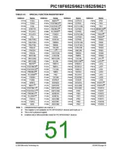
PIC18F6525/6621/8525/8621
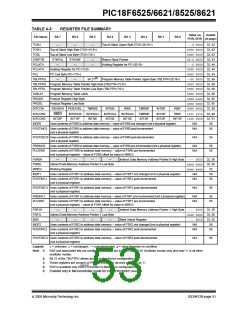
TABLE 4-3:
File Name
REGISTER FILE SUMMARY (CONTINUED)
Value on
POR, BOR on page:
Details
Bit 7
Bit 6
Bit 5
Bit 4
Bit 3
Bit 2
Bit 1
Bit 0
CMCON
C2OUT
C1OUT
C2INV
C1INV
CIS
CM2
CM1
CM0
0000 0000 34, 243
xxxx xxxx 34, 145
xxxx xxxx 34, 145
TMR3H
TMR3L
T3CON
PSPCON
SPBRG1
RCREG1
TXREG1
TXSTA1
RCSTA1
EEADRH
EEADR
EEDATA
EECON2
EECON1
IPR3
Timer3 Register High Byte
Timer3 Register Low Byte
RD16
IBF
T3CCP2
OBF
T3CKPS1
IBOV
T3CKPS0
T3CCP1
—
T3SYNC
—
TMR3CS
—
TMR3ON 0000 0000 34, 145
(5)
PSPMODE
—
0000 ---- 34, 129
0000 0000 34, 217
0000 0000 34, 224
0000 0000 34, 222
0000 0010 34, 214
0000 000x 34, 215
Enhanced USART1 Baud Rate Generator Register Low Byte
Enhanced USART1 Receive Register
Enhanced USART1 Transmit Register
CSRC
SPEN
—
TX9
RX9
—
TXEN
SREN
—
SYNC
CREN
—
SENDB
ADDEN
—
BRGH
FERR
—
TRMT
OERR
TX9D
RX9D
EE Addr Register High ---- --00 34, 83
0000 0000 34, 83
Data EEPROM Address Register
Data EEPROM Data Register
0000 0000 34, 83
Data EEPROM Control Register 2 (not a physical register)
---- ---- 34, 83
EEPGD
—
CFGS
—
—
FREE
TX2IP
TX2IF
TX2IE
EEIP
WRERR
TMR4IP
TMR4IF
TMR4IE
BCLIP
BCLIF
BCLIE
SSPIP
SSPIF
SSPIE
—
WREN
CCP5IP
CCP5IF
CCP5IE
LVDIP
WR
RD
xx-0 x000 34, 80
RC2IP
RC2IF
RC2IE
—
CCP4IP
CCP4IF
CCP4IE
TMR3IP
TMR3IF
TMR3IE
TMR2IP
TMR2IF
TMR2IE
WM1
CCP3IP --11 1111 35, 100
CCP3IF --00 0000 35, 94
CCP3IE --00 0000 35, 97
CCP2IP -1-1 1111 35, 99
CCP2IF -0-0 0000 35, 93
CCP2IE -0-0 0000 35, 96
TMR1IP 1111 1111 35, 98
TMR1IF 0000 0000 35, 92
TMR1IE 0000 0000 35, 95
PIR3
—
—
PIE3
—
—
IPR2
—
CMIP
CMIF
CMIE
ADIP
ADIF
ADIE
—
PIR2
—
—
EEIF
LVDIF
PIE2
—
—
EEIE
LVDIE
(5)
IPR1
PSPIP
RC1IP
RC1IF
RC1IE
WAIT1
TX1IP
TX1IF
TX1IE
WAIT0
CCP1IP
CCP1IF
CCP1IE
—
(5)
PIR1
PSPIF
(5)
PIE1
PSPIE
(3)
MEMCON
EBDIS
WM0
0-00 --00 35, 71
1111 1111 35, 127
1111 1111 35, 124
---1 1111 35, 119
1111 1111 35, 116
1111 1111 35, 113
1111 1111 35, 110
1111 1111 35, 108
1111 1111 35, 105
-111 1111 35, 121
xxxx xxxx 35, 127
xxxx xxxx 35, 124
---x xxxx 35, 121
xxxx xxxx 35, 119
xxxx xxxx 35, 116
xxxx xxxx 35, 113
xxxx xxxx 35, 110
xxxx xxxx 35, 108
-xxx xxxx 35, 105
(3)
TRISJ
Data Direction Control Register for PORTJ
Data Direction Control Register for PORTH
(3)
TRISH
TRISG
TRISF
TRISE
TRISD
TRISC
TRISB
TRISA
—
—
—
Data Direction Control Register for PORTG
Data Direction Control Register for PORTF
Data Direction Control Register for PORTE
Data Direction Control Register for PORTD
Data Direction Control Register for PORTC
Data Direction Control Register for PORTB
(1)
—
TRISA6
Data Direction Control Register for PORTA
(3)
LATJ
Read PORTJ Data Latch, Write PORTJ Data Latch
Read PORTH Data Latch, Write PORTH Data Latch
(3)
LATH
LATG
LATF
LATE
LATD
LATC
LATB
LATA
—
—
—
Read PORTG Data Latch, Write PORTG Data Latch
Read PORTF Data Latch, Write PORTF Data Latch
Read PORTE Data Latch, Write PORTE Data Latch
Read PORTD Data Latch, Write PORTD Data Latch
Read PORTC Data Latch, Write PORTC Data Latch
Read PORTB Data Latch, Write PORTB Data Latch
(1)
(1)
—
LATA6
Read PORTA Data Latch, Write PORTA Data Latch
Legend:
Note 1:
x= unknown, u= unchanged, – = unimplemented, q= value depends on condition
RA6 and associated bits are configured as a port pin in RCIO and ECIO Oscillator modes only and read ‘0’ in all other
oscillator modes.
2:
3:
4:
Bit 21 of the TBLPTRU allows access to the device configuration bits.
These registers are unused on PIC18F6525/6621 devices and read as ‘0’.
RG5 is available only if MCLR function is disabled in configuration.
5: Enabled only in Microcontroller mode for PIC18F8525/8621 devices.
2005 Microchip Technology Inc.
DS39612B-page 53

 MICROCHIP [ MICROCHIP ]