PIC18F6525/6621/8525/8621
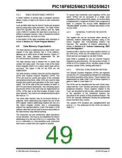
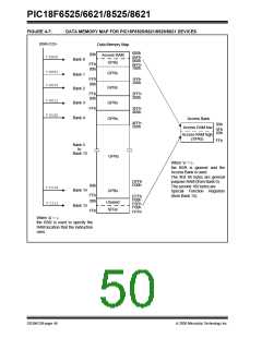
FIGURE 4-7:
DATA MEMORY MAP FOR PIC18F6525/6621/8525/8621 DEVICES
BSR<3:0>
Data Memory Map
000h
00h
Access RAM
GPRs
= 0000
05Fh
Bank 0
060h
FFh
00h
0FFh
100h
= 0001
= 0010
GPRs
GPRs
Bank 1
Bank 2
Bank 3
FFh
00h
1FFh
200h
FFh
00h
2FFh
300h
= 0011
= 0100
GPRs
GPRs
FFh
3FFh
400h
Bank 4
Access Bank
4FFh
500h
00h
Access RAM low
5Fh
60h
Access RAM high
(SFRs)
FFh
Bank 5
to
Bank 13
GPRs
GPRs
When ‘a’ = 0,
the BSR is ignored and the
Access Bank is used.
The first 96 bytes are general
purpose RAM (from Bank 0).
The second 160 bytes are
Special Function Registers
(from Bank 15).
DFFh
E00h
00h
= 1110
Bank 14
Bank 15
FFh
00h
EFFh
F00h
Unused
SFRs
= 1111
F5Fh
F60h
FFh
FFFh
When ‘a’ = 1,
the BSR is used to specify the
RAM location that the instruction
uses.
DS39612B-page 48
2005 Microchip Technology Inc.

 MICROCHIP [ MICROCHIP ]