PIC18F6525/6621/8525/8621
To ensure that commonly used registers (SFRs and
select GPRs) can be accessed in a single cycle
regardless of the current BSR values, an Access Bank
is implemented. A segment of Bank 0 and a segment of
Bank 15 comprise the Access RAM. Section 4.10
“Access Bank” provides a detailed description of the
Access RAM.
4.8.2
TABLE READS/TABLE WRITES
A better method of storing data in program memory
allows 2 bytes of data to be stored in each instruction
location.
Look-up table data may be stored 2 bytes per program
word by using table reads and writes. The Table Pointer
(TBLPTR) specifies the byte address and the Table
Latch (TABLAT) contains the data that is read from, or
written to program memory. Data is transferred to/from
program memory, one byte at a time.
4.9.1
GENERAL PURPOSE REGISTER
FILE
The register file can be accessed either directly or
indirectly. Indirect addressing operates using a File
Select Register and corresponding Indirect File
Operand. The operation of indirect addressing is
shown in Section 4.12 “Indirect Addressing, INDF
and FSR Registers”.
A description of the table read/table write operation is
shown in Section 5.0 “Flash Program Memory”.
4.9
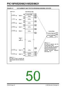
Data Memory Organization
The data memory is implemented as static RAM. Each
register in the data memory has a 12-bit address,
allowing up to 4096 bytes of data memory. Figure 4-7
shows the data memory organization for the
PIC18F6525/6621/8525/8621 devices.
Enhanced MCU devices may have banked memory in
the GPR area. GPRs are not initialized by a Power-on
Reset and are unchanged on all other Resets.
Data RAM is available for use as General Purpose
Registers by all instructions. The top section of Bank 15
(F60h to FFFh) contains SFRs. All other banks of data
memory contain GPRs, starting with Bank 0.
The data memory map is divided into 16 banks that
contain 256 bytes each. The lower 4 bits of the Bank
Select Register (BSR<3:0>) select which bank will be
accessed. The upper 4 bits for the BSR are not
implemented.
4.9.2
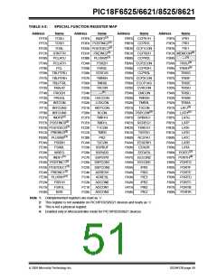
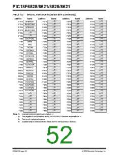
SPECIAL FUNCTION REGISTERS
The Special Function Registers (SFRs) are registers
used by the CPU and peripheral modules for controlling
the desired operation of the device. These registers are
implemented as static RAM. A list of these registers is
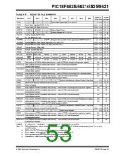
given in Table 4-2 and Table 4-3.
The data memory contains Special Function Registers
(SFR) and General Purpose Registers (GPR). The
SFRs are used for control and status of the controller
and peripheral functions, while GPRs are used for data
storage and scratch pad operations in the user’s appli-
cation. The SFRs start at the last location of Bank 15
(0FFFh) and extend downwards. Any remaining space
beyond the SFRs in the bank may be implemented as
GPRs. GPRs start at the first location of Bank 0 and
grow upwards. Any read of an unimplemented location
will read as ‘0’s.
The SFRs can be classified into two sets: those asso-
ciated with the “core” function and those related to the
peripheral functions. Those registers related to the
“core” are described in this section, while those related
to the operation of the peripheral features are
described in the section of that peripheral feature. The
SFRs are typically distributed among the peripherals
whose functions they control.
The entire data memory may be accessed directly or
indirectly. Direct addressing may require the use of the
BSR register. Indirect addressing requires the use of a
File Select Register (FSRn) and a corresponding
Indirect File Operand (INDFn). Each FSR holds a 12-bit
address value that can be used to access any location in
the data memory map without banking.
The unused SFR locations are unimplemented and
read as ‘0’s. The addresses for the SFRs are listed in
Table 4-2.
The instruction set and architecture allow operations
across all banks. This may be accomplished by indirect
addressing or by the use of the MOVFFinstruction. The
MOVFF instruction is a two-word/two-cycle instruction
that moves a value from one register to another.
2005 Microchip Technology Inc.
DS39612B-page 47

 MICROCHIP [ MICROCHIP ]