PIC18F6525/6621/8525/8621
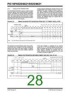
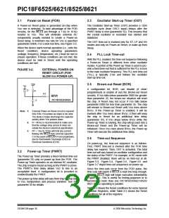
A timing diagram indicating the transition from the main
oscillator to the Timer1 oscillator is shown in Figure 2-8.
The Timer1 oscillator is assumed to be running all the
time. After the SCS0 bit is set, the processor is frozen at
the next occurring Q1 cycle. After eight synchronization
cycles are counted from the Timer1 oscillator, operation
resumes. No additional delays are required after the
synchronization cycles.
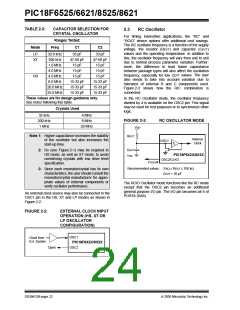
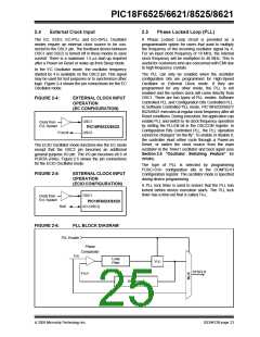
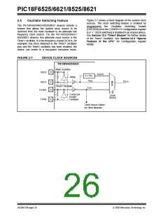
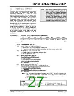
2.6.2
OSCILLATOR TRANSITIONS
PIC18F6525/6621/8525/8621 devices contain circuitry
to prevent “glitches” when switching between oscillator
sources. Essentially, the circuitry waits for eight rising
edges of the clock source that the processor is switch-
ing to. This ensures that the new clock source is stable
and that its pulse width will not be less than the shortest
pulse width of the two clock sources.
FIGURE 2-8:
TIMING DIAGRAM FOR TRANSITION FROM OSC1 TO TIMER1 OSCILLATOR
Q1 Q2 Q3 Q4 Q1
Q1
Q2
Q3
Q4
Q1
Q2
Q3
Q4
Q1
TT1P
2
1
3
4
5
6
7
8
T1OSI
OSC1
TSCS
Internal
System
Clock
TOSC
TDLY
SCS
(OSCCON<0>)
Program
Counter
PC
PC + 2
PC + 4
Note: TDLY is the delay from SCS high to first count of transition circuit.
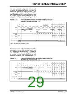
The sequence of events that takes place when switch-
ing from the Timer1 oscillator to the main oscillator will
depend on the mode of the main oscillator. In addition
to eight clock cycles of the main oscillator, additional
delays may take place.
If the main oscillator is configured for an external
crystal (HS, XT, LP), then the transition will take place
after an oscillator start-up time (TOST) has occurred. A
timing diagram, indicating the transition from the
Timer1 oscillator to the main oscillator for HS, XT and
LP modes, is shown in Figure 2-9.
FIGURE 2-9:
TIMING FOR TRANSITION BETWEEN TIMER1 AND OSC1 (HS, XT, LP)
Q1 Q2 Q3 Q4 Q1 Q2 Q3
Q3
Q4
Q1
TT1P
T1OSI
OSC1
1
2
3
4
5
6
7
8
TOST
TSCS
TOSC
Internal
System Clock
SCS
(OSCCON<0>)
Program
Counter
PC
PC + 2
PC + 6
Note: TOST = 1024 TOSC (drawing not to scale).
DS39612B-page 26
2005 Microchip Technology Inc.

 MICROCHIP [ MICROCHIP ]