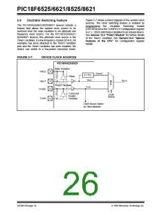
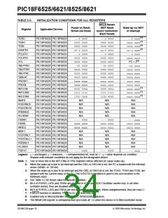
PIC18F6525/6621/8525/8621
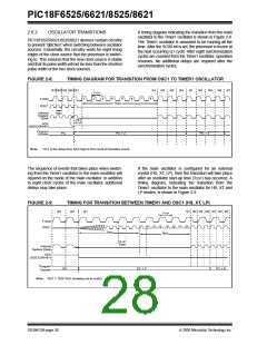
If the main oscillator is configured in the RC, RCIO, EC
or ECIO modes, there is no oscillator start-up time-out.
Operation will resume after eight cycles of the main
oscillator have been counted. A timing diagram, indi-
cating the transition from the Timer1 oscillator to the
main oscillator for RC, RCIO, EC and ECIO modes, is
shown in Figure 2-12.
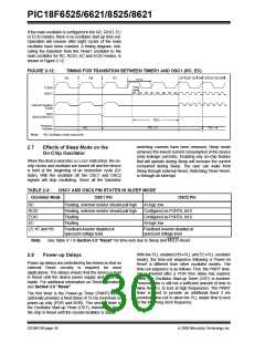
FIGURE 2-12:
TIMING FOR TRANSITION BETWEEN TIMER1 AND OSC1 (RC, EC)
Q3
Q4
Q1
Q1 Q2 Q3 Q4 Q1 Q2 Q3 Q4
TT1P
TOSC
T1OSI
OSC1
1
2
3
4
5
6
7
8
Internal System
Clock
SCS
(OSCCON<0>)
TSCS
Program
Counter
PC + 2
PC
PC + 4
Note:
RC Oscillator mode assumed.
switching currents have been removed, Sleep mode
achieves the lowest current consumption of the device
(only leakage currents). Enabling any on-chip feature
that will operate during Sleep will increase the current
consumed during Sleep. The user can wake from
Sleep through external Reset, Watchdog Timer Reset,
or through an interrupt.
2.7
Effects of Sleep Mode on the
On-Chip Oscillator
When the device executes a SLEEPinstruction, the on-
chip clocks and oscillator are turned off and the device
is held at the beginning of an instruction cycle (Q1
state). With the oscillator off, the OSC1 and OSC2
signals will stop oscillating. Since all the transistor
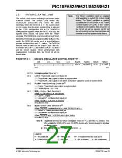
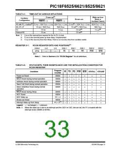
TABLE 2-3:
OSC1 AND OSC2 PIN STATES IN SLEEP MODE
OSC1 Pin
Oscillator Mode
OSC2 Pin
RC
Floating, external resistor should pull high
At logic low
RCIO
Floating, external resistor should pull high
Configured as PORTA, bit 6
Configured as PORTA, bit 6
At logic low
ECIO
Floating
Floating
EC
LP, XT and HS
Feedback inverter disabled at
quiescent voltage level
Feedback inverter disabled at
quiescent voltage level
Note:
See Table 3-1 in Section 3.0 “Reset” for time-outs due to Sleep and MCLR Reset.
With the PLL enabled (HS+PLL and EC+PLL oscillator
2.8
Power-up Delays
mode), the time-out sequence following a Power-on
Reset is different from other oscillator modes. The
time-out sequence is as follows: First, the PWRT time-
out is invoked after a POR time delay has expired.
Then, the Oscillator Start-up Timer (OST) is invoked.
However, this is still not a sufficient amount of time to
allow the PLL to lock at high frequencies. The PWRT
timer is used to provide an additional fixed 2 ms
(nominal) time-out to allow the PLL ample time to lock
to the incoming clock frequency.
Power-up delays are controlled by two timers so that no
external Reset circuitry is required for most
applications. The delays ensure that the device is kept
in Reset until the device power supply and clock are
stable. For additional information on Reset operation,
see Section 3.0 “Reset”.
The first timer is the Power-up Timer (PWRT) which
optionally provides a fixed delay of 72 ms (nominal) on
power-up only (POR and BOR). The second timer is
the Oscillator Start-up Timer (OST), intended to keep
the chip in Reset until the crystal oscillator is stable.
DS39612B-page 28
2005 Microchip Technology Inc.

 MICROCHIP [ MICROCHIP ]