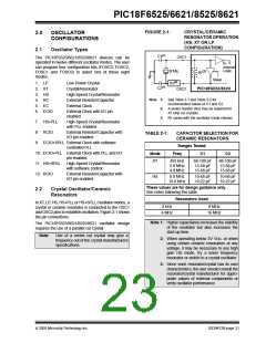
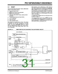
PIC18F6525/6621/8525/8621
2.6.1
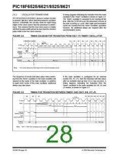
SYSTEM CLOCK SWITCH BIT
Note:
The Timer1 oscillator must be enabled
and operating to switch the system clock
source. The Timer1 oscillator is enabled
by setting the T1OSCEN bit in the Timer1
Control register (T1CON). If the Timer1
oscillator is not enabled, then any write to
the SCS0 bit will be ignored (SCS0 bit
forced cleared) and the main oscillator will
continue to be the system clock source.
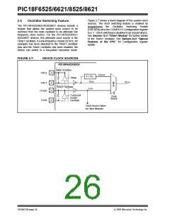
The system clock source switching is performed under
software control. The system clock switch bits,
SCS1:SCS0 (OSCCON<1:0>), control the clock
switching. When the SCS0 bit is ‘0’, the system clock
source comes from the main oscillator that is selected
by the FOSC configuration bits in the CONFIG1H
Configuration register. When the SCS0 bit is set, the
system clock source will come from the Timer1
oscillator. The SCS0 bit is cleared on all forms of Reset.
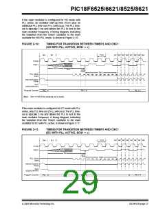
When the FOSC bits are programmed for Software PLL
mode, the SCS1 bit can be used to select between
primary oscillator/clock and PLL output. The SCS1 bit
will only have an effect on the system clock if the PLL
is enabled (PLLEN = 1) and locked (LOCK = 1), else it
will be forced cleared. When programmed with
Configuration Controlled PLL, the SCS1 bit will be
forced clear.
REGISTER 2-1:
OSCCON: OSCILLATOR CONTROL REGISTER
U-0
—
U-0
—
U-0
—
U-0
—
R/W-0
LOCK
R/W-0
PLLEN(1)
R/W-0
SCS1
R/W-0
SCS0(2)
bit 7
bit 0
bit 7-4 Unimplemented: Read as ‘0’
bit 3
bit 2
bit 1
LOCK: Phase Lock Loop Lock Status bit
1= Phase Lock Loop output is stable as system clock
0= Phase Lock Loop output is not stable and output cannot be used as system clock
PLLEN: Phase Lock Loop Enable bit(1)
1= Enable Phase Lock Loop output as system clock
0= Disable Phase Lock Loop
SCS1: System Clock Switch bit 1
When PLLEN and LOCK bits are set:
1= Use PLL output
0= Use primary oscillator/clock input pin
When PLLEN or LOCK bit is cleared:
Bit is forced clear.
bit 0
SCS0: System Clock Switch bit 0(2)
When OSCSEN configuration bit = 0and T1OSCEN bit = 1:
1= Switch to Timer1 oscillator/clock pin
0= Use primary oscillator/clock input pin
When OSCSEN and T1OSCEN are in other states:
Bit is forced clear.
Note 1: PLLEN bit is forced set when configured for ECIO+PLL and HS+PLL modes. This
bit is writable for ECIO+SPLL and HS+SPLL modes only; forced cleared for all other
oscillator modes.
2: The setting of SCS0 = 1supersedes SCS1 = 1.
Legend:
R = Readable bit
-n = Value at POR
W = Writable bit
‘1’ = Bit is set
U = Unimplemented bit, read as ‘0’
‘0’ = Bit is cleared x = Bit is unknown
2005 Microchip Technology Inc.
DS39612B-page 25

 MICROCHIP [ MICROCHIP ]