PIC18F6525/6621/8525/8621
3.1
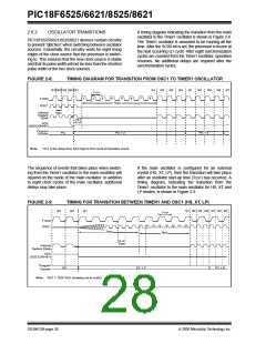
Power-on Reset (POR)
3.3
Oscillator Start-up Timer (OST)
A Power-on Reset pulse is generated on-chip when
VDD rise is detected. To take advantage of the POR
circuitry, tie the MCLR pin through a 1 kΩ to 10 kΩ
resistor to VDD. This will eliminate external RC
components usually needed to create a Power-on
Reset delay. A minimum rise rate for VDD is specified
(parameter D004). For a slow rise time, see Figure 3-2.
The Oscillator Start-up Timer (OST) provides a 1024
oscillator cycle (from OSC1 input) delays after the
PWRT delay is over (parameter 32). This ensures that
the crystal oscillator or resonator has started and
stabilized.
The OST time-out is invoked only for XT, LP and HS
modes and only on Power-on Reset, or wake-up from
Sleep.
When the device starts normal operation (i.e., exits the
Reset condition), device operating parameters
(voltage, frequency, temperature, etc.) must be met to
ensure operation. If these conditions are not met, the
device must be held in Reset until the operating
conditions are met.
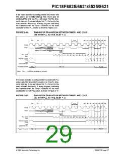
3.4
PLL Lock Time-out
With the PLL enabled, the time-out sequence following
a Power-on Reset is different from other oscillator
modes. A portion of the Power-up Timer is used to pro-
vide a fixed time-out that is sufficient for the PLL to lock
to the main oscillator frequency. This PLL lock time-out
(TPLL) is typically 2 ms and follows the oscillator
start-up time-out.
FIGURE 3-2:
EXTERNAL POWER-ON
RESET CIRCUIT (FOR
SLOW VDD POWER-UP)
VDD
3.5
Brown-out Reset (BOR)
A configuration bit, BOR, can disable (if clear/
programmed) or enable (if set) the Brown-out Reset
circuitry. If VDD falls below parameter D005 for greater
than parameter 35, the brown-out situation will reset
the chip. A Reset may not occur if VDD falls below
parameter D005 for less than parameter 35. The chip
will remain in Brown-out Reset until VDD rises above
BVDD. If the Power-up Timer is enabled, it will be
invoked after VDD rises above BVDD; it then will keep
the chip in Reset for an additional time delay
(parameter 33). If VDD drops below BVDD while the
Power-up Timer is running, the chip will go back into a
Brown-out Reset and the Power-up Timer will be
initialized. Once VDD rises above BVDD, the Power-up
Timer will execute the additional time delay.
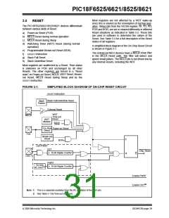
D
R
R1
MCLR
PIC18F6X2X/8X2X
C
Note 1: External Power-on Reset circuit is required
only if the VDD power-up slope is too slow.
The diode D helps discharge the capacitor
quickly when VDD powers down.
2: R < 40 kΩ is recommended to make sure
that the voltage drop across R does not
violate the device’s electrical specification.
3: R1 = 1 kΩ to 10 kΩ will limit any current
flowing into MCLR from external capacitor
C in the event of MCLR/VPP pin breakdown,
due to Electrostatic Discharge (ESD) or
Electrical Overstress (EOS).
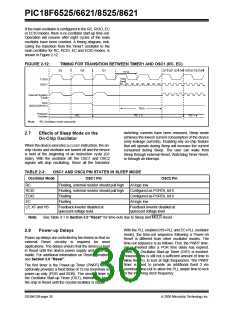
3.6
Time-out Sequence
On power-up, the time-out sequence is as follows:
First, PWRT time-out is invoked after the POR time
delay has expired. Then, OST is activated. The total
time-out will vary based on oscillator configuration and
the status of the PWRT. For example, in RC mode with
the PWRT disabled, there will be no time-out at all.
Figure 3-3, Figure 3-4, Figure 3-5, Figure 3-6 and
Figure 3-7 depict time-out sequences on power-up.
3.2
Power-up Timer (PWRT)
The Power-up Timer provides a fixed nominal time-out
(parameter 33) only on power-up from the POR. The
Power-up Timer operates on an internal RC oscillator.
The chip is kept in Reset as long as the PWRT is active.
The PWRT’s time delay allows VDD to rise to an
acceptable level. A configuration bit is provided to
enable/disable the PWRT.
Since the time-outs occur from the POR pulse, the
time-outs will expire if MCLR is kept low long enough.
Bringing MCLR high will begin execution immediately
(Figure 3-5). This is useful for testing purposes or to
synchronize more than one PIC18F6525/6621/8525/
8621 device operating in parallel.
The power-up time delay will vary from chip-to-chip due
to VDD, temperature and process variation. See DC
parameter 33 for details.
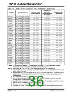
Table 3-2 shows the Reset conditions for some Special
Function Registers, while Table 3-3 shows the Reset
conditions for all of the registers.
DS39612B-page 30
2005 Microchip Technology Inc.

 MICROCHIP [ MICROCHIP ]