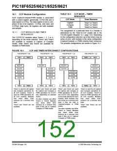
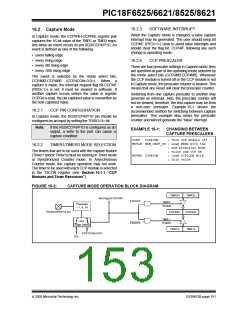
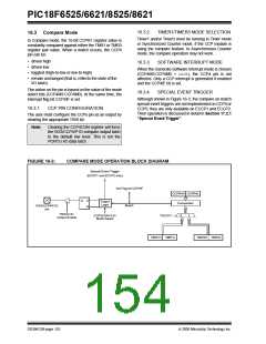
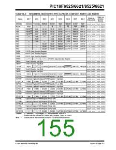
PIC18F6525/6621/8525/8621
16.4.1
PWM PERIOD
16.4 PWM Mode
The PWM period is specified by writing to the PR2
(PR4) register. The PWM period can be calculated
using the following formula:
In Pulse-Width Modulation (PWM) mode, the CCP4 pin
produces up to a 10-bit resolution PWM output. Since
the CCP4 pin is multiplexed with the PORTG data
latch, the TRISG<3> bit must be cleared to make the
CCP4 pin an output.
EQUATION 16-1:
PWM Period = [(PR2) + 1] • 4 • TOSC •
(TMR2 Prescale Value)
Note:
Clearing the CCP4CON register will force
the CCP4 PWM output latch to the default
low level. This is not the PORTG I/O data
latch.
PWM frequency is defined as 1/[PWM period].
When TMR2 (TMR4) is equal to PR2 (PR2), the
following three events occur on the next increment
cycle:
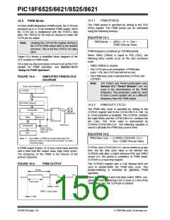
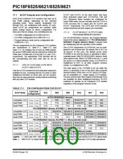
Figure 16-4 shows a simplified block diagram of the
CCP module in PWM mode.
For a step-by-step procedure on how to set up the CCP
module for PWM operation, see Section 16.4.3
“Setup for PWM Operation”.
• TMR2 (TMR4) is cleared
• The CCP4 pin is set (exception: if PWM duty
cycle = 0%, the CCP4 pin will not be set)
• The PWM duty cycle is latched from CCPR4L into
CCPR4H
FIGURE 16-4:
SIMPLIFIED PWM BLOCK
DIAGRAM
Note:
The Timer2 and Timer4 postscalers (see
Section 13.0 “Timer2 Module”) are not
used in the determination of the PWM
frequency. The postscaler could be used
to have a servo update rate at a different
frequency than the PWM output.
CCP1CON<5:4>
Duty Cycle Registers
CCPR4L
CCPR4H (Slave)
Comparator
16.4.2
PWM DUTY CYCLE
The PWM duty cycle is specified by writing to the
CCPR4L register and to the CCP4CON<5:4> bits. Up
to 10-bit resolution is available. The CCPR4L contains
the eight MSbs and the CCP4CON<5:4> contains the
two LSbs. This 10-bit value is represented by
CCPR4L:CCP4CON<5:4>. The following equation is
used to calculate the PWM duty cycle in time:
Q
R
S
RG3/CCP4
(Note 1)
TMR2
TRISG<3>
Comparator
PR2
Clear Timer,
CCP1 pin and
latch D.C.
EQUATION 16-2:
PWM Duty Cycle = (CCPR4L:CCP4CON<5:4>) •
TOSC • (TMR2 Prescale Value)
Note 1: 8-bit TMR2 or TMR4 is concatenated with 2-bit
internal Q clock, or 2 bits of the prescaler, to create
10-bit time base.
CCPR4L and CCP4CON<5:4> can be written to at any
time, but the duty cycle value is not latched into
CCPR4H until after a match between PR2 and TMR2
occurs (i.e., the period is complete). In PWM mode,
CCPR4H is a read-only register.
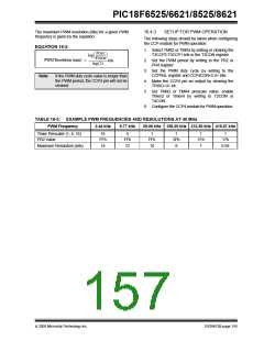
A PWM output (Figure 16-5) has a time base (period)
and a time that the output stays high (duty cycle).
The frequency of the PWM is the inverse of the
period (1/period).
FIGURE 16-5:
PWM OUTPUT
The CCPR4H register and a 2-bit internal latch are
used to double-buffer the PWM duty cycle. This
double-buffering is essential for glitchless PWM
operation.
Period
When the CCPR4H and 2-bit latch match TMR2, con-
catenated with an internal 2-bit Q clock or 2 bits of the
TMR2 prescaler, the CCP4 pin is cleared.
Duty Cycle
TMR2 = PR2
TMR2 = Duty Cycle
TMR2 = PR2
DS39612B-page 154
2005 Microchip Technology Inc.

 MICROCHIP [ MICROCHIP ]