PIC18F6525/6621/8525/8621
ECCP1 and ECCP3, on the other hand, only have
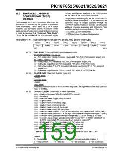
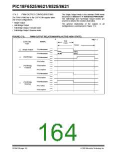
17.1 ECCP Outputs and Configuration
three dedicated output pins: ECCPx/PxA, PxB and
PxC. Whenever these modules are configured for
Quad PWM mode, the pin normally used for CCP4 or
CCP5 becomes the D output pins for ECCP3 and
ECCP1, respectively. The CCP4 and CCP5 modules
remain functional but their outputs are overridden.
Each of the Enhanced CCP modules may have up to
four PWM outputs, depending on the selected
operating mode. These outputs, designated PxA
through PxD, are multiplexed with various I/O pins.
Some ECCP pin assignments are constant, while
others change based on device configuration. For
those pins that do change, the controlling bits are:
17.1.2
ECCP MODULE OUTPUTS AND
PROGRAM MEMORY MODES
• CCP2MX configuration bit (CONFIG3H<0>)
• ECCPMX configuration bit (CONFIG3H<1>)
For PIC18F8525/8621 devices, the Program Memory
mode of the device (Section 4.1.1 “PIC18F6525/6621/
8525/8621 Program Memory Modes”) impacts both
pin multiplexing and the operation of the module.
• Program Memory mode (set by configuration bits
CONFIG3L<1:0>)
The pin assignments for the Enhanced CCP modules
are summarized in Table 17-1, Table 17-2 and
Table 17-3. To configure the I/O pins as PWM outputs,
the proper PWM mode must be selected by setting the
PxMx and CCPxMx bits (CCPxCON<7:6> and <3:0>,
respectively). The appropriate TRIS direction bits for
the corresponding port pins must also be set as
outputs.
The ECCP2 input/output (ECCP2/P2A) can be multi-
plexed to one of three pins. By default, this is RC1 for
all devices. In this case, the default occurs when
CCP2MX is set and the device is operating in Micro-
controller mode. With PIC18F8525/8621 devices, three
other options exist. When CCP2MX is not set (= 0) and
the device is in Microcontroller mode, ECCP2/P2A is
multiplexed to RE7; in all other program memory
modes, it is multiplexed to RB3.
17.1.1
USE OF CCP4 AND CCP5 WITH
ECCP1 AND ECCP3
The final option is for CCP2MX to be set while the
device is operating in one of the three other program
memory modes. In this case, ECCP1 and ECCP3 oper-
ate as compatible (i.e., single output) CCP modules.
The pins used by their other outputs (PxB through PxD)
are available for other multiplexed functions. ECCP2
continues to operate as an Enhanced CCP module
regardless of the program memory mode.
Only the ECCP2 module has four dedicated output pins
available for use. Assuming that the I/O ports or other
multiplexed functions on those pins are not needed,
they may be used whenever needed without interfering
with any other CCP module.
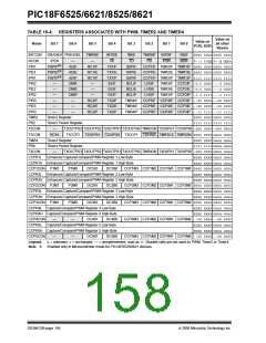
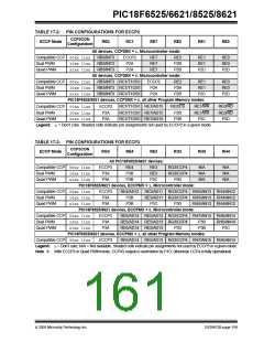
TABLE 17-1: PIN CONFIGURATIONS FOR ECCP1
CCP1CON
ECCP Mode
RC2
RE6
RE5
RG4
RH7
RH6
Configuration
All PIC18F6525/6621 devices:
Compatible CCP 00xx 11xx
ECCP1
P1A
RE6
P1B
P1B
RE5
RE5
P1C
RG4/CCP5
RG4/CCP5
P1D
N/A
N/A
N/A
N/A
N/A
N/A
Dual PWM
Quad PWM
10xx 11xx
x1xx 11xx
P1A
PIC18F8525/8621 devices, ECCPMX = 1, Microcontroller mode:
Compatible CCP 00xx 11xx
ECCP1
P1A
RE6/AD14 RE5/AD13 RG4/CCP5 RH7/AN15 RH6/AN14
Dual PWM
Quad PWM
10xx 11xx
x1xx 11xx
P1B
P1B
RE5/AD13 RG4/CCP5 RH7/AN15 RH6/AN14
P1A
P1C
P1D
RH7/AN15 RH6/AN14
PIC18F8525/8621 devices, ECCPMX = 0, Microcontroller mode:
Compatible CCP 00xx 11xx
ECCP1
P1A
RE6/AD14 RE5/AD13 RG4/CCP5 RH7/AN15 RH6/AN14
Dual PWM
Quad PWM
10xx 11xx
x1xx 11xx
RE6/AD14 RE5/AD13 RG4/CCP5
RE6/AD14 RE5/AD13 P1D
P1B
P1B
RH6/AN14
P1C
P1A
PIC18F8525/8621 devices, ECCPMX = 1, all other Program Memory modes:
Compatible CCP 00xx 11xx
ECCP1
RE6/AD14 RE5/AD13 RG4/CCP5 RH7/AN15 RH6/AN14
Legend: x= Don’t care, N/A = Not available. Shaded cells indicate pin assignments not used by ECCP1 in a given mode.
Note 1: With ECCP1 in Quad PWM mode, CCP5’s output is overridden by P1D; otherwise CCP5 is fully operational.
DS39612B-page 158
2005 Microchip Technology Inc.

 MICROCHIP [ MICROCHIP ]