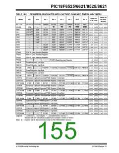
PIC18F6525/6621/8525/8621
16.3.2
TIMER1/TIMER3 MODE SELECTION
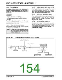
16.3 Compare Mode
Timer1 and/or Timer3 must be running in Timer mode
or Synchronized Counter mode, if the CCP module is
using the compare feature. In Asynchronous Counter
mode, the compare operation may not work.
In Compare mode, the 16-bit CCPR1 register value is
constantly compared against either the TMR1 or TMR3
register pair value. When a match occurs, the CCP4
pin can be:
• driven high
16.3.3
SOFTWARE INTERRUPT MODE
• driven low
When the Generate Software Interrupt mode is chosen
(CCP4M3:CCP4M0 = 1010), the CCP4 pin is not
affected. Only a CCP interrupt is generated if enabled
and the CCP4IE bit is set.
• toggled (high-to-low or low-to-high)
• remain unchanged (that is, reflects the state of the
I/O latch)
The action on the pin is based on the value of the mode
select bits (CCP4M3:CCP4M0). At the same time, the
interrupt flag bit CCP4IF is set.
16.3.4
SPECIAL EVENT TRIGGER
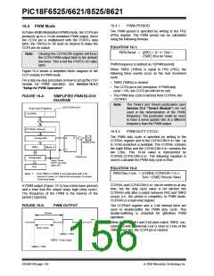
Although shown in Figure 16-3, the compare on match
special event triggers are not implemented on CCP4 or
CCP5; they are only available on ECCP1 and ECCP2.
Their operation is discussed in detail in Section 17.2.1
“Special Event Trigger”.
16.3.1
CCP PIN CONFIGURATION
The user must configure the CCPx pin as an output by
clearing the appropriate TRIS bit.
Note:
Clearing the CCP4CON register will force
the RG3/CCP4/P1D compare output latch
to the default low level. This is not the
PORTG I/O data latch.
FIGURE 16-3:
COMPARE MODE OPERATION BLOCK DIAGRAM
Special Event Trigger
(ECCP1 and ECCP2 only)
Set Flag bit CCP4IF
CCPR4H CCPR4L
Comparator
Q
S
R
Output
Logic
Match
RG3/CCP4/P1D
pin
TRISG<3>
Output Enable
1
CCP4CON<3:0>
Mode Select
0
T3CCP2
TMR1H TMR1L
TMR3H TMR3L
DS39612B-page 152
2005 Microchip Technology Inc.

 MICROCHIP [ MICROCHIP ]