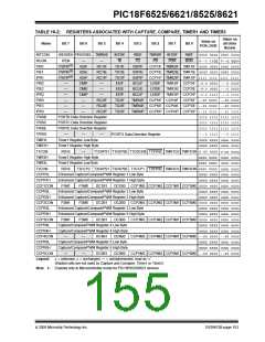
PIC18F6525/6621/8525/8621
Capture and Compare functions of the ECCP module
are the same as the standard CCP module.
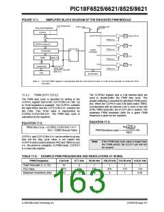
17.0 ENHANCED CAPTURE/
COMPARE/PWM (ECCP)
MODULE
The prototype control register for the Enhanced CCP
module is shown in Register 17-1. In addition to the
The Enhanced CCP (ECCP) modules differ from the
standard CCP modules by the addition of Enhanced
PWM capabilities. These allow for 2 or 4 output
channels, user selectable polarity, dead-band control
and automatic shutdown and restart and are discussed
in detail in Section 17.4 “Enhanced PWM Mode”.
Except for the addition of the special event trigger,
expanded range of modes available through the
CCPxCON register, the ECCP modules each have two
additional registers associated with Enhanced PWM
operation and auto-shutdown features. They are:
• ECCPxDEL (Dead-Band Delay)
• ECCPxAS (Auto-Shutdown Configuration)
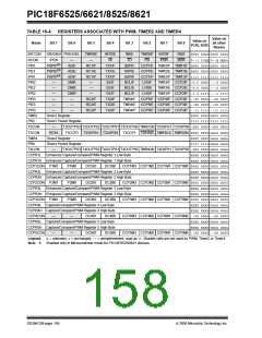
REGISTER 17-1: CCPxCON REGISTER (ECCP1, ECCP2 AND ECCP3 MODULES)
R/W-0
PxM1
R/W-0
PxM0
R/W-0
R/W-0
R/W-0
R/W-0
R/W-0
R/W-0
DCxB1
DCxB0
CCPxM3 CCPxM2 CCPxM1 CCPxM0
bit 0
bit 7
bit 7-6
PxM1:PxM0: Enhanced PWM Output Configuration bits
If CCPxM3:CCPxM2 = 00, 01, 10:
xx= PxA assigned as Capture/Compare input/output; PxB, PxC, PxD assigned as port pins
If CCPxM3:CCPxM2 = 11:
00= Single output: PxA modulated; PxB, PxC, PxD assigned as port pins
01= Full-bridge output forward: P1D modulated; P1A active; P1B, P1C inactive
10= Half-bridge output: P1A, P1B modulated with dead-band control; P1C, P1D assigned
as port pins
11= Full-bridge output reverse: P1B modulated; P1C active; P1A, P1D inactive
bit 5-4
DCxB1:DCxB0: PWM Duty Cycle bit 1 and bit 0
Capture mode:
Unused.
Compare mode:
Unused.
PWM mode:
These bits are the two LSbs of the 10-bit PWM duty cycle. The eight MSbs of the duty cycle are
found in CCPRxL.
bit 3-0
CCPxM3:CCPxM0: Enhanced CCP Mode Select bits
0000= Capture/Compare/PWM off (resets ECCPx module)
0001= Reserved
0010= Compare mode, toggle output on match
0011= Capture mode
0100= Capture mode, every falling edge
0101= Capture mode, every rising edge
0110= Capture mode, every 4th rising edge
0111= Capture mode, every 16th rising edge
1000= Compare mode, initialize ECCP pin low, set output on compare match (set CCPxIF)
1001= Compare mode, initialize ECCP pin high, clear output on compare match (set CCPxIF)
1010= Compare mode, generate software interrupt only, ECCP pin reverts to I/O state
1011= Compare mode, trigger special event (ECCP resets TMR1 or TMR3, sets CCxIF bit,
ECCP2 trigger starts A/D conversion if A/D module is enabled)(1)
1100= PWM mode; PxA, PxC active-high; PxB, PxD active-high
1101= PWM mode; PxA, PxC active-high; PxB, PxD active-low
1110= PWM mode; PxA, PxC active-low; PxB, PxD active-high
1111= PWM mode; PxA, PxC active-low; PxB, PxD active-low
Note 1: Implemented only for ECCP1 and ECCP2; same as ‘1010’ for ECCP3.
Legend:
R = Readable bit
-n = Value at POR
W = Writable bit
‘1’ = Bit is set
U = Unimplemented bit, read as ‘0’
‘0’ = Bit is cleared x = Bit is unknown
2005 Microchip Technology Inc.
DS39612B-page 157

 MICROCHIP [ MICROCHIP ]