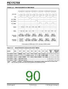
PIC17C75X
13.1.1.1 EXTERNAL CLOCK INPUT FOR TIMER1
AND TIMER2
13.1
Timer1 and Timer2
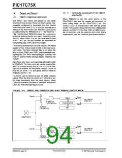
13.1.1 TIMER1, TIMER2 IN 8-BIT MODE
When TMRxCS is set, the clock source is the
RB4/TCLK12 pin, and the counter will increment on
every falling edge on the RB4/TCLK12 pin. The
TCLK12 input is synchronized with internal phase
clocks.This causes a delay from the time a falling edge
appears on TCLK12 to the time TMR1 or TMR2 is actu-
ally incremented. For the external clock input timing
requirements, see the Electrical Specification section.
Both Timer1 and Timer2 will operate in 8-bit mode
when the T16 bit is clear.These two timers can be inde-
pendently configured to increment from the internal
instruction cycle clock (TCY) or from an external clock
source on the RB4/TCLK12 pin.The timer clock source
is configured by the TMRxCS bit (x = 1 for Timer1 or =
2 for Timer2). When TMRxCS is clear, the clock source
is internal and increments once every instruction cycle
(Fosc/4). When TMRxCS is set, the clock source is the
RB4/TCLK12 pin, and the counters will increment on
every falling edge of the RB4/TCLK12 pin.
The timer increments from 00h until it equals the Period
register (PRx). It then resets to 00h at the next incre-
ment cycle. The timer interrupt flag is set when the
timer is reset. TMR1 and TMR2 have individual inter-
rupt flag bits. The TMR1 interrupt flag bit is latched into
TMR1IF, and the TMR2 interrupt flag bit is latched into
TMR2IF.
Each timer also has a corresponding interrupt enable
bit (TMRxIE). The timer interrupt can be enabled/dis-
abled by setting/clearing this bit. For peripheral inter-
rupts to be enabled, the Peripheral Interrupt Enable bit
must be set (PEIE = '1') and global interrupt must be
enabled (GLINTD = '0').
The timers can be turned on and off under software
control. When the timer on control bit (TMRxON) is set,
the timer increments from the clock source. When
TMRxON is cleared, the timer is turned off and cannot
cause the timer interrupt flag to be set.
FIGURE 13-4: TIMER1 AND TIMER2 IN TWO 8-BIT TIMER/COUNTER MODE
0
1
Fosc/4
Reset
Equal
TMR1
CCoommppaarraatotorr<x88>
PR1
Set TMR1IF
(PIR1<4>)
TMR1ON
(TCON2<0>)
TMR1CS
(TCON1<0>)
RB4/TCLK12
1
0
Reset
Equal
TMR2
CCoommppaarraatotorr<x88>
PR2
Set TMR2IF
(PIR1<5>)
Fosc/4
TMR2ON
(TCON2<1>)
TMR2CS
(TCON1<1>)
DS30264A-page 94
Preliminary
1997 Microchip Technology Inc.

 MICROCHIP [ MICROCHIP ]