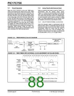
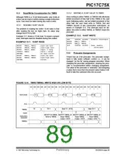
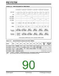
PIC17C75X
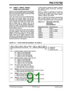
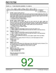
FIGURE 13-2: TCON2 REGISTER (ADDRESS: 17h, BANK 3)
R - 0
R - 0
R/W - 0
R/W - 0 R/W - 0 R/W - 0 R/W - 0 R/W - 0
R = Readable bit
W = Writable bit
-n = Value at POR reset
CA2OVF CA1OVF PWM2ON PWM1ON CA1/PR3 TMR3ON TMR2ON TMR1ON
bit7
bit0
bit 7:
CA2OVF: Capture2 Overflow Status bit
This bit indicates that the capture value had not been read from the capture register pair (CA2H:CA2L)
before the next capture event occurred.The capture register retains the oldest unread capture value (last
capture before overflow). Subsequent capture events will not update the capture register with the TMR3
value until the capture register has been read (both bytes).
1 = Overflow occurred on Capture2 register
0 = No overflow occurred on Capture2 register
bit 6:
CA1OVF: Capture1 Overflow Status bit
This bit indicates that the capture value had not been read from the capture register pair
(PR3H/CA1H:PR3L/CA1L) before the next capture event occurred. The capture register retains the old-
est unread capture value (last capture before overflow). Subsequent capture events will not update the
capture register with the TMR3 value until the capture register has been read (both bytes).
1 = Overflow occurred on Capture1 register
0 = No overflow occurred on Capture1 register
bit 5:
bit 4:
bit 3:
PWM2ON: PWM2 On bit
1 = PWM2 is enabled (The RB3/PWM2 pin ignores the state of the DDRB<3> bit)
0 = PWM2 is disabled (The RB3/PWM2 pin uses the state of the DDRB<3> bit for data direction)
PWM1ON: PWM1 On bit
1 = PWM1 is enabled (The RB2/PWM1 pin ignores the state of the DDRB<2> bit)
0 = PWM1 is disabled (The RB2/PWM1 pin uses the state of the DDRB<2> bit for data direction)
CA1/PR3: CA1/PR3 Register Mode Select bit
1 = Enables Capture1 (PR3H/CA1H:PR3L/CA1L is the Capture1 register. Timer3 runs without
a period register)
0 = Enables the Period register (PR3H/CA1H:PR3L/CA1L is the Period register for Timer3)
bit 2:
bit 1:
TMR3ON: Timer3 On bit
1 = Starts Timer3
0 = Stops Timer3
TMR2ON: Timer2 On bit
This bit controls the incrementing of the TMR2 register. When TMR2:TMR1 form the 16-bit timer (T16 is
set), TMR2ON must be set. This allows the MSB of the timer to increment.
1 = Starts Timer2 (Must be enabled if the T16 bit (TCON1<3>) is set)
0 = Stops Timer2
bit 0:
TMR1ON: Timer1 On bit
When T16 is set (in 16-bit Timer Mode)
1 = Starts 16-bit TMR2:TMR1
0 = Stops 16-bit TMR2:TMR1
When T16 is clear (in 8-bit Timer Mode)
1 = Starts 8-bit Timer1
0 = Stops 8-bit Timer1
DS30264A-page 92
Preliminary
1997 Microchip Technology Inc.

 MICROCHIP [ MICROCHIP ]