PIC17C75X
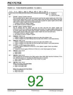
Six other registers comprise the Capture2, Capture3,
and Capture4 registers (CA2H:CA2L, CA3H:CA3L,
and CA4H:CA4L).
13.0 TIMER1, TIMER2, TIMER3,
PWMS AND CAPTURES
The PIC17C75X has a wealth of timers and time-based
functions to ease the implementation of control applica-
tions. These time-base functions include three PWM
outputs and four Capture inputs.
Figure 13-1, Figure 13-2, and Figure 13-3 are the con-
trol registers for the operation of Timer1, Timer2, and
Timer3, as well as PWM1, PWM2, PWM3, Capture1,
Capture2, Capture3, and Capture4.
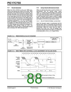
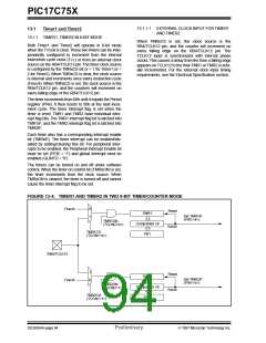
Timer1 and Timer2 are two 8-bit incrementing timers,
each with an 8-bit period register (PR1 and PR2
respectively) and separate overflow interrupt flags.
Timer1 and Timer2 can operate either as timers (incre-
ment on internal Fosc/4 clock) or as counters (incre-
ment on falling edge of external clock on pin
RB4/TCLK12). They are also software configurable to
operate as a single 16-bit timer/counter. These timers
are also used as the time-base for the PWM (Pulse
Width Modulation) modules.
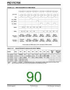
Table 13-1 shows the Timer resource requirements for
these time-base functions. Each timer is an open
resource so that multiple functions may operate with it.
TABLE 13-1: TIME-BASE FUNCTION /
RESOURCE
REQUIREMENTS
Time-base Function
PWM1
Timer Resource
Timer1
Timer3 is a 16-bit timer/counter which uses the TMR3H
and TMR3L registers. Timer3 also has two additional
registers (PR3H/CA1H: PR3L/CA1L) that are config-
urable as a 16-bit period register or a 16-bit capture
register. TMR3 can be software configured to incre-
ment from the internal system clock (FOSC/4) or from
an external signal on the RB5/TCLK3 pin.Timer3 is the
time-base for all of the 16-bit captures.
PWM2
Timer1 or Timer2
Timer1 or Timer2
Timer3
PWM3
Capture1
Capture2
Capture3
Capture4
Timer3
Timer3
Timer3
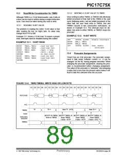
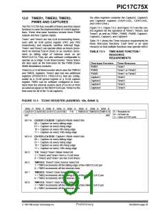
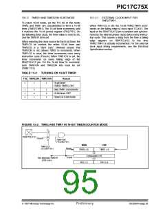
FIGURE 13-1: TCON1 REGISTER (ADDRESS: 16h, BANK 3)
R/W - 0 R/W - 0 R/W - 0 R/W - 0 R/W - 0 R/W - 0 R/W - 0 R/W - 0
R = Readable bit
W = Writable bit
-n = Value at POR reset
CA2ED1 CA2ED0 CA1ED1 CA1ED0
T16
TMR3CS TMR2CS TMR1CS
bit7
bit0
bit 7-6: CA2ED1:CA2ED0: Capture2 Mode Select bits
00 = Capture on every falling edge
01 = Capture on every rising edge
10 = Capture on every 4th rising edge
11 = Capture on every 16th rising edge
bit 5-4: CA1ED1:CA1ED0: Capture1 Mode Select bits
00 = Capture on every falling edge
01 = Capture on every rising edge
10 = Capture on every 4th rising edge
11 = Capture on every 16th rising edge
bit 3:
bit 2:
bit 1:
bit 0:
T16: Timer2:Timer1 Mode Select bit
1 = Timer2 and Timer1 form a 16-bit timer
0 = Timer2 and Timer1 are two 8-bit timers
TMR3CS: Timer3 Clock Source Select bit
1 = TMR3 increments off the falling edge of the RB5/TCLK3 pin
0 = TMR3 increments off the internal clock
TMR2CS: Timer2 Clock Source Select bit
1 = TMR2 increments off the falling edge of the RB4/TCLK12 pin
0 = TMR2 increments off the internal clock
TMR1CS: Timer1 Clock Source Select bit
1 = TMR1 increments off the falling edge of the RB4/TCLK12 pin
0 = TMR1 increments off the internal clock
1997 Microchip Technology Inc.
Preliminary
DS30264A-page 91

 MICROCHIP [ MICROCHIP ]