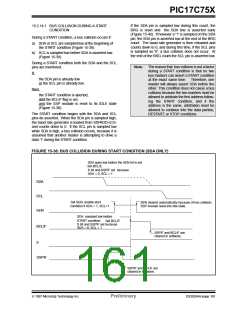
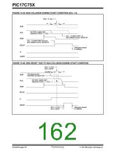
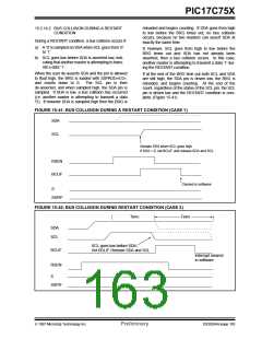
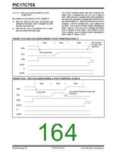
PIC17C75X
2
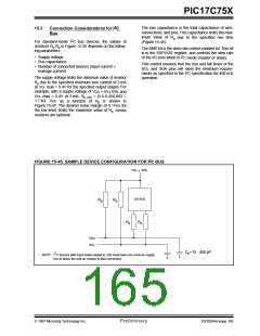
The bus capacitance is the total capacitance of wire,
connections, and pins.This capacitance limits the max-
15.3
Connection Considerations for I C
Bus
imum value of R due to the specified rise time
p
2
For standard-mode I C bus devices, the values of
(Figure 15-45).
resistors R R in Figure 15-45 depends on the follow-
ing parameters
p
s
The SMP bit is the slew rate control enabled bit.This bit
is in the SSPSTAT register, and controls the slew rate
of the I/O pins when in I C mode (master or slave).
2
• Supply voltage
• Bus capacitance
• Number of connected devices (input current +
leakage current).
This control ensures that the rise and fall times of the
SCL and SDA pins will meet the minimum require-
ments as specified in the I C specification for 400 kHz
2
The supply voltage limits the minimum value of resistor
operation.
R due to the specified minimum sink current of 3 mA
p
at VOL max = 0.4V for the specified output stages. For
example, with a supply voltage of VDD = 5V+10% and
VOL max = 0.4V at 3 mA, R
= (5.5-0.4)/0.003 =
p min
1.7 kΩ. VDD as a function of R is shown in
p
Figure 15-45. The desired noise margin of 0.1VDD for
the low level, limits the maximum value of R . Series
s
resistors are optional.
2
FIGURE 15-45: SAMPLE DEVICE CONFIGURATION FOR I C BUS
VDD + 10%
DEVICE
R
R
p
p
R
R
s
s
SDA
SCL
C =10 - 400 pF
2
b
NOTE: I C devices with input levels related to VDD must have one common supply
line to which the pull up resistor is also connected.
1997 Microchip Technology Inc.
Preliminary
DS30264A-page 165

 MICROCHIP [ MICROCHIP ]