PIC16F87/88
12.2 Selecting the A/D Conversion
Clock
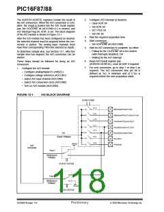
12.3 Configuring Analog Port Pins
The ADCON1, ANSEL, TRISA, and TRISB registers
control the operation of the A/D port pins. The port pins
that are desired as analog inputs must have their cor-
responding TRIS bits set (input). If the TRIS bit is
cleared (output), the digital output level (VOH or VOL)
will be converted.
The A/D conversion time per bit is defined as TAD. The
A/D conversion requires 9.0 TAD per 8-bit conversion.
The source of the A/D conversion clock is software
selectable. The seven possible options for TAD are:
• 2 TOSC
The A/D operation is independent of the state of the
CHS<2:0> bits and the TRIS bits.
• 4 TOSC
• 8 TOSC
Note 1: When reading the port register, all pins
configured as analog input channels will
read as cleared (a low level). Pins config-
ured as digital inputs will convert an ana-
log input. Analog levels on a digitally
configured input will not affect the
conversion accuracy.
• 16 TOSC
• 32 TOSC
• 64 TOSC
• Internal A/D module RC oscillator (2-6 µs)
For correct A/D conversions, the A/D conversion clock
(TAD) must be selected to ensure a minimum TAD time
as small as possible, but no less than 1.6 µs and not
greater than 6.4 µs.
2: Analog levels on any pin that is defined as
a digital input (including the RA4:RA0 and
RB7:RB6 pins), may cause the input
buffer to consume current out of the
device specification.
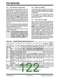
Table 12-1 shows the resultant TAD times derived from
the device operating frequencies and the A/D clock
source selected.
TABLE 12-1: TAD vs. MAXIMUM DEVICE OPERATING FREQUENCIES – STANDARD DEVICES (C)
AD Clock Source (TAD)
ADCS<2>
Maximum Device Frequency
Max.
Operation
ADCS<1:0>
2 TOSC
4 TOSC
0
1
0
1
0
1
X
00
00
01
01
10
10
11
1.25 MHz
2.5 MHz
5 MHz
8 TOSC
16 TOSC
32 TOSC
64 TOSC
RC(1,2,3)
10 MHz
20 MHz
20 MHz
(Note 1)
Note 1: The RC source has a typical TAD time of 4 µs, but can vary between 2-6 µs.
2: When the device frequencies are greater than 1 MHz, the RC A/D conversion clock source is only
recommended for SLEEP operation.
3: For extended voltage devices (LF), please refer to Section 18.0 “Electrical Characteristics”.
DS30487B-page 118
Preliminary
2003 Microchip Technology Inc.

 MICROCHIP [ MICROCHIP ]