PIC16F87/88
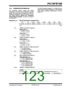
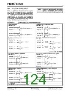
13.1 Comparator Configuration
Note:
Comparator interrupts should be disabled
during Comparator mode change.
Otherwise, a false interrupt may occur.
a
There are eight modes of operation for the compara-
tors. The CMCON register is used to select these
modes. Figure 13-1 shows the eight possible modes.
The TRISA register controls the data direction of the
comparator pins for each mode. If the Comparator
mode is changed, the comparator output level may not
be valid for the specified mode change delay shown in
Section 18.0 “Electrical Characteristics”.
FIGURE 13-1:
COMPARATOR I/O OPERATING MODES
Comparators Reset
Comparators Off (POR Default Value)
CM2:CM0 = 000
CM2:CM0 = 111
A
D
VIN-
VIN-
RA0/AN0
RA0/AN0
Off (Read as ‘0’)
Off (Read as ‘0’)
Off (Read as ‘0’)
C1
C1
VIN+
VIN+
A
D
RA3/AN3
RA3/AN3
A
D
VIN-
VIN-
RA1/AN1
RA1/AN1
Off (Read as ‘0’)
C2
C2
VIN+
VIN+
A
D
RA2/AN2
RA2/AN2
Four Inputs Multiplexed to Two Comparators
Two Independent Comparators
CM2:CM0 = 010
CM2:CM0 = 100
A
A
VIN-
RA0/AN0
RA0/AN0
RA3/AN3
CIS = 0
CIS = 1
VIN-
C1OUT
C2OUT
C1
C2
VIN+
A
A
RA3/AN3
C1OUT
C2OUT
C1
C2
VIN+
A
A
RA1/AN1
RA2/AN2
VIN-
CIS = 0
CIS = 1
A
A
VIN-
RA1/AN1
RA2/AN2
VIN+
VIN+
From VREF Module
Two Common Reference Comparators with Outputs
Two Common Reference Comparators
CM2:CM0 = 110
CM2:CM0 = 011
A
VIN-
A
VIN-
RA0/AN0
RA3/AN3
RA0/AN0
RA3/AN3
C1OUT
C2OUT
C1OUT
C2OUT
C1
C2
C1
C2
VIN+
VIN+
D
D
A
A
VIN-
A
A
VIN-
RA1/AN1
RA2/AN2
RA1/AN1
RA2/AN2
VIN+
VIN+
RA4/T0CKI
One Independent Comparator
Three Inputs Multiplexed to Two Comparators
CM2:CM0 = 101
CM2:CM0 = 001
D
VIN-
A
RA0/AN0
RA3/AN3
RA0/AN0
CIS = 0
CIS = 1
VIN-
Off (Read as ‘0’)
C1
C2
VIN+
D
A
RA3/AN3
C1OUT
C2OUT
C1
C2
VIN+
A
A
A
A
VIN-
VIN-
RA1/AN1
RA2/AN2
RA1/AN1
RA2/AN2
C2OUT
VIN+
VIN+
A = Analog Input, port reads zeros always.
D = Digital Input.
CIS (CMCON<3>) is the Comparator Input Switch.
DS30487B-page 122
Preliminary
2003 Microchip Technology Inc.

 MICROCHIP [ MICROCHIP ]