PIC16F87/88
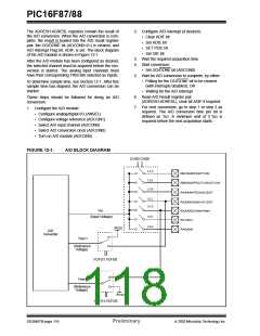
The ADRESH:ADRESL registers contain the result of
the A/D conversion. When the A/D conversion is com-
plete, the result is loaded into the A/D result register
pair, the GO/DONE bit (ADCON0<2>) is cleared, and
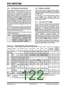
A/D Interrupt Flag bit, ADIF, is set. The block diagram
of the A/D module is shown in Figure 12-1.
2. Configure A/D interrupt (if desired):
• Clear ADIF bit
• Set ADIE bit
• SET PEIE bit
• Set GIE bit
3. Wait the required acquisition time.
4. Start conversion:
After the A/D module has been configured as desired,
the selected channel must be acquired before the con-
version is started. The analog input channels must
have their corresponding TRIS bits selected as inputs.
• Set GO/DONE bit (ADCON0)
5. Wait for A/D conversion to complete, by either:
• Polling for the GO/DONE bit to be cleared
(with interrupts disabled); OR
To determine sample time, see Section 12.1. After this
sample time has elapsed, the A/D conversion can be
started.
• Waiting for the A/D interrupt
6. Read A/D Result register pair
These steps should be followed for doing an A/D
conversion:
(ADRESH:ADRESL), clear bit ADIF if required.
7. For next conversion, go to step 1 or step 2 as
required. The A/D conversion time per bit is
defined as TAD. A minimum wait of 2 TAD is
required before the next acquisition starts.
1. Configure the A/D module:
• Configure analog/digital I/O (ANSEL)
• Configure voltage reference (ADCON1)
• Select A/D input channel (ADCON0)
• Select A/D conversion clock (ADCON0)
• Turn on A/D module (ADCON0)
FIGURE 12-1:
A/D BLOCK DIAGRAM
CHS2:CHS0
110
RB7/AN6/PGD/T1OSI
101
RB6/AN5/PGC/T1OSO/T1CKI
100
RA4/AN4/T0CKI/C2OUT
011
RA3/AN3/VREF+/C1OUT
010
VIN
RA2/AN2/CVREF/VREF-
001
(Input Voltage)
RA1/AN1
000
AVDD
RA0/AN0
A/D
Converter
VREF+
(Reference
Voltage)
VCFG1:VCFG0
VREF-
(Reference
Voltage)
AVSS
VCFG1:VCFG0
DS30487B-page 116
Preliminary
2003 Microchip Technology Inc.

 MICROCHIP [ MICROCHIP ]