PIC16F87/88
may be decreased. After the analog input channel is
selected (changed), this acquisition must be done
before the conversion can be started.
12.1 A/D Acquisition Requirements
For the A/D converter to meet its specified accuracy,
the charge holding capacitor (CHOLD) must be allowed
to fully charge to the input channel voltage level. The
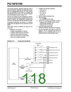
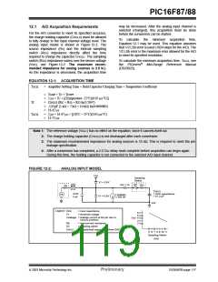
analog input model is shown in Figure 12-2. The
source impedance (RS) and the internal sampling
switch (RSS) impedance directly affect the time
required to charge the capacitor CHOLD. The sampling
switch (RSS) impedance varies over the device voltage
(VDD), see Figure 12-2. The maximum recom-
mended impedance for analog sources is 2.5 kΩ.
As the impedance is decreased, the acquisition time
To calculate the minimum acquisition time,
Equation 12-1 may be used. This equation assumes
that 1/2 LSb error is used (1024 steps for the A/D). The
1/2 LSb error is the maximum error allowed for the A/D
to meet its specified resolution.
To calculate the minimum acquisition time, TACQ, see
the PICmicro® Mid-Range Reference Manual
(DS33023).
EQUATION 12-1: ACQUISITION TIME
TACQ
= Amplifier Settling Time + Hold Capacitor Charging Time + Temperature Coefficient
= TAMP + TC + TCOFF
= 2 µs + TC + [(Temperature -25°C)(0.05 µs/°C)]
= CHOLD (RIC + RSS + RS) In(1/2047)
= -120 pF (1 kΩ + 7 kΩ + 10 kΩ) In(0.0004885)
= 16.47 µs
= 2 µs + 16.47 µs + [(50°C – 25°C)(0.05 µs/°C)
= 19.72 µs
TC
TACQ
Note 1: The reference voltage (VREF) has no effect on the equation, since it cancels itself out.
2: The charge holding capacitor (CHOLD) is not discharged after each conversion.
3: The maximum recommended impedance for analog sources is 10 kΩ. This is required to meet the pin
leakage specification.
4: After a conversion has completed, a 2.0 TAD delay must complete before acquisition can begin again.
During this time, the holding capacitor is not connected to the selected A/D input channel.
FIGURE 12-2:
ANALOG INPUT MODEL
VDD
Sampling
Switch
VT = 0.6V
ANx
SS
RIC ≤ 1k
RSS
Rs
CHOLD
= DAC capacitance
= 51.2 pF
CPIN
5 pF
VA
I leakage
500 nA
VT = 0.6V
VSS
Legend:
CPIN
VT
= input capacitance
= threshold voltage
6 V
5 V
I leakage = leakage current at the pin due to
various junctions
RIC
VDD 4 V
3 V
2 V
= interconnect resistance
= sampling switch
SS
CHOLD
= sample/hold capacitance (from DAC)
5 6 7 8 9 10 11
Sampling Switch
(kΩ)
2003 Microchip Technology Inc.
Preliminary
DS30487B-page 117

 MICROCHIP [ MICROCHIP ]