PIC16F87/88
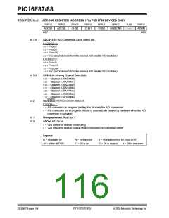
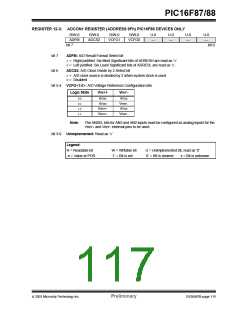
REGISTER 12-3: ADCON1 REGISTER (ADDRESS 9Fh) PIC16F88 DEVICES ONLY
R/W-0
ADFM
R/W-0
R/W-0
R/W-0
U-0
—
U-0
—
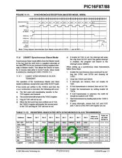
U-0
—
U-0
—
ADCS2
VCFG1
VCFG0
bit 7
bit 0
bit 7
bit 6
ADFM: A/D Result Format Select bit
1= Right justified. Six Most Significant bits of ADRESH are read as ‘0’.
0= Left justified. Six Least Significant bits of ADRESL are read as ‘0’.
ADCS2: A/D Clock Divide by 2 Select bit
1= A/D clock source is divided by 2 when system clock is used
0= Disabled
bit 5-4 VCFG<1:0>: A/D Voltage Reference Configuration bits
Logic State
VREF+
VREF-
00
01
10
11
AVDD
AVDD
AVSS
VREF-
AVSS
VREF+
VREF+
VREF-
Note:
The ANSEL bits for AN3 and AN2 inputs must be configured as analog inputs for the
VREF+ and VREF- external pins to be used.
bit 3-0 Unimplemented: Read as ‘0’
Legend:
R = Readable bit
-n = Value at POR
W = Writable bit
‘1’ = Bit is set
U = Unimplemented bit, read as ‘0’
‘0’ = Bit is cleared x = Bit is unknown
2003 Microchip Technology Inc.
Preliminary
DS30487B-page 115

 MICROCHIP [ MICROCHIP ]