PIC16F87/88
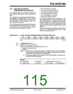
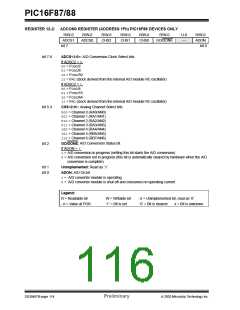
REGISTER 12-2: ADCON0 REGISTER (ADDRESS 1Fh) PIC16F88 DEVICES ONLY
R/W-0
ADCS1
bit 7
R/W-0
R/W-0
CHS2
R/W-0
CHS1
R/W-0
CHS0
R/W-0
U-0
—
R/W-0
ADON
bit 0
ADCS0
GO/DONE
bit 7-6
ADCS<1:0>: A/D Conversion Clock Select bits
If ADSC2 = 0:
00= FOSC/2
01= FOSC/8
10= FOSC/32
11= FRC (clock derived from the internal A/D module RC oscillator)
If ADSC2 = 1:
00= FOSC/4
01= FOSC/16
10= FOSC/64
11= FRC (clock derived from the internal A/D module RC oscillator)
bit 5-3
CHS<2:0>: Analog Channel Select bits
000= Channel 0 (RA0/AN0)
001= Channel 1 (RA1/AN1)
010= Channel 2 (RA2/AN2)
011= Channel 3 (RA3/AN3)
100= Channel 4 (RA4/AN4)
101= Channel 5 (RB6/AN5)
110= Channel 6 (RB7/AN6)
bit 2
GO/DONE: A/D Conversion Status bit
If ADON = 1:
1= A/D conversion in progress (setting this bit starts the A/D conversion)
0= A/D conversion not in progress (this bit is automatically cleared by hardware when the A/D
conversion is complete)
bit 1
bit 0
Unimplemented: Read as ‘0’
ADON: A/D On bit
1= A/D converter module is operating
0= A/D converter module is shut-off and consumes no operating current
Legend:
R = Readable bit
W = Writable bit
‘1’ = Bit is set
U = Unimplemented bit, read as ‘0’
‘0’ = Bit is cleared x = Bit is unknown
- n = Value at POR
DS30487B-page 114
Preliminary
2003 Microchip Technology Inc.

 MICROCHIP [ MICROCHIP ]