PIC16F87/88
12.4.1
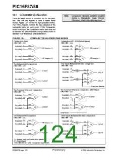
A/D RESULT REGISTERS
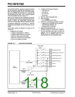
12.4 A/D Conversions
The ADRESH:ADRESL register pair is the location
where the 10-bit A/D result is loaded at the completion
of the A/D conversion. This register pair is 16 bits wide.
The A/D module gives the flexibility to left or right justify
the 10-bit result in the 16-bit result register. The A/D
Format Select bit (ADFM) controls this justification.
Figure 12-4 shows the operation of the A/D result
justification. The extra bits are loaded with ‘0’s. When
an A/D result will not overwrite these locations (A/D dis-
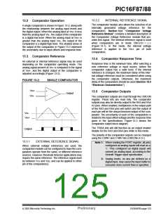
able), these registers may be used as two general
purpose 8-bit registers.
Clearing the GO/DONE bit during a conversion will
abort the current conversion. The A/D result register
pair will NOT be updated with the partially completed
A/D conversion sample. That is, the ADRESH:ADRESL
registers will continue to contain the value of the last
completed conversion (or the last value written to the
ADRESH:ADRESL registers). After the A/D conversion
is aborted, a 2 TAD wait is required before the next
acquisition is started. After this 2 TAD wait, acquisition
on the selected channel is automatically started. The
GO/DONE bit can then be set to start the conversion.
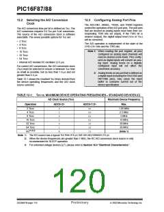
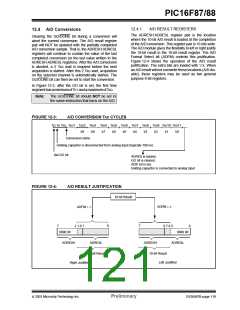
In Figure 12-3, after the GO bit is set, the first time
segmenthasaminimumofTCY andamaximumofTAD.
Note:
The GO/DONE bit should NOT be set in
the same instruction that turns on the A/D.
FIGURE 12-3:
A/D CONVERSION TAD CYCLES
TCY to TAD
TAD1 TAD2 TAD3 TAD4 TAD5 TAD6
T
AD
7
T
AD
8
TAD9 TAD10 TAD11
b2 b1 b0
b9
b8
b7
b6
b5
b4
b3
Conversion starts
Holding capacitor is disconnected from analog input (typically 100 ns)
Set GO bit
ADRES is loaded,
GO bit is cleared,
ADIF bit is set,
holding capacitor is connected to analog input
FIGURE 12-4:
A/D RESULT JUSTIFICATION
10-bit Result
ADFM = 0
ADFM = 1
0
7
7
2 1 0 7
0 7 6 5
0
0000 00
0000 00
ADRESH
ADRESL
ADRESH
ADRESL
10-bit Result
Right Justified
10-bit Result
Left Justified
2003 Microchip Technology Inc.
Preliminary
DS30487B-page 119

 MICROCHIP [ MICROCHIP ]