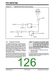
PIC16F87/88
12.5 A/D Operation During SLEEP
12.6 Effects of a RESET
The A/D module can operate during SLEEP mode. This
requires that the A/D clock source be set to RC
(ADCS1:ADCS0 = 11). When the RC clock source is
selected, the A/D module waits one instruction cycle
before starting the conversion. This allows the SLEEP
instruction to be executed, which eliminates all digital
switching noise from the conversion. When the conver-
sion is completed, the GO/DONE bit will be cleared and
the result loaded into the ADRES register. If the A/D
interrupt is enabled, the device will wake-up from
SLEEP. If the A/D interrupt is not enabled, the A/D mod-
ule will then be turned off, although the ADON bit will
remain set.
A device RESET forces all registers to their RESET
state. The A/D module is disabled and any conversion
in progress is aborted. All A/D input pins are configured
as analog inputs.
The value that is in the ADRESH:ADRESL registers
is not modified for
a
Power-on Reset. The
ADRESH:ADRESL registers will contain unknown data
after a Power-on Reset.
12.7 Use of the CCP Trigger
An A/D conversion can be started by the “special event
trigger” of the CCP module. This requires that the
CCP1M3:CCP1M0 bits (CCP1CON<3:0>) be pro-
grammed as ‘1011’ and that the A/D module is enabled
(ADON bit is set). When the trigger occurs, the GO/
DONE bit will be set, starting the A/D conversion and
the Timer1 counter will be reset to zero. Timer1 is reset
to automatically repeat the A/D acquisition period with
When the A/D clock source is another clock option (not
RC), a SLEEPinstruction will cause the present conver-
sion to be aborted and the A/D module to be turned off,
though the ADON bit will remain set.
Turning off the A/D places the A/D module in its lowest
current consumption state.
minimal
software
overhead
(moving
the
ADRESH:ADRESL to the desired location). The appro-
priate analog input channel must be selected and the
minimum acquisition done before the “special event
trigger” sets the GO/DONE bit (starts a conversion).
Note:
For the A/D module to operate in SLEEP,
the A/D clock source must be set to RC
(ADCS1:ADCS0 = 11). To perform an A/D
conversion in SLEEP, ensure the SLEEP
instruction immediately follows the
instruction that sets the GO/DONE bit.
If the A/D module is not enabled (ADON is cleared), then
the “special event trigger” will be ignored by the A/D
module, but will still reset the Timer1 counter.
TABLE 12-2: REGISTERS/BITS ASSOCIATED WITH A/D
Value on
all other
RESETS
Value on
POR, BOR
Address
Name
Bit 7
Bit 6
Bit 5
Bit 4
Bit 3
Bit 2
Bit 1
Bit 0
0Bh, 8Bh INTCON
10Bh, 18Bh
GIE
PEIE
TMR0IE INTE
RBIE
TMR0IF
INTF
RBIF
0000 000x 0000 000u
0Ch
8Ch
1Eh
9Eh
1Fh
9Fh
9Bh
05h
PIR1
—
—
ADIF
ADIE
RCIF
RCIE
TXIF SSPIF CCP1IF TMR2IF TMR1IF -000 0000 -000 0000
TXIE SSPIE CCP1IE TMR2IE TMR1IE -000 0000 -000 0000
xxxx xxxx uuuu uuuu
PIE1
(1)
ADRESH
A/D Result Register High Byte
A/D Result Register Low Byte
(1)
(1)
ADRESL
xxxx xxxx uuuu uuuu
ADCON0
ADCS1 ADCS0
CHS2
CHS1 CHS0 GO/DONE
—
—
ADON 0000 00-0 0000 00-0
(1)
ADCON1
ADFM ADCS2 VCFG1 VCFG0
—
—
—
0000 ---- 0000 ----
-111 1111 -111 1111
(1)
ANSEL
—
AN6
RA6
AN5
RA5
AN4
RA4
AN3
RA3
AN2
RA2
AN1
RA1
AN0
RA0
PORTA
RA7
(PIC16F87)
(PIC16F88)
xxxx 0000 uuuu 0000
xxx0 0000 uuu0 0000
05h, 106h PORTB
(PIC16F87)
RB7
RB6
RB5
RB4
RB3
RB2
RB1
RB0
xxxx xxxx uuuu uuuu
00xx xxxx 00uu uuuu
(PIC16F88)
(2)
85h
TRISA
TRISA7 TRISA6 TRISA5 PORTA Data Direction Register
1111 1111 1111 1111
86h, 186h TRISB
Legend: x= unknown, u= unchanged, - = unimplemented, read as ‘0’. Shaded cells are not used for A/D conversion.
Note 1: PIC16F88 only.
2: Pin 5 is an input only; the state of the TRISA5 bit has no effect and will always read ‘1’.
TRISB7 TRISB6 TRISB5 TRISB4 TRISB3 TRISB2 TRISB1 TRISB0 1111 1111 1111 1111
DS30487B-page 120
Preliminary
2003 Microchip Technology Inc.

 MICROCHIP [ MICROCHIP ]