PIC16F87/88
The A/D module has five registers:
12.0 ANALOG-TO-DIGITAL
CONVERTER (A/D) MODULE
• A/D Result High Register (ADRESH)
• A/D Result Low Register (ADRESL)
• A/D Control Register 0 (ADCON0)
• A/D Control Register 1 (ADCON1)
• Analog Select Register (ANSEL)
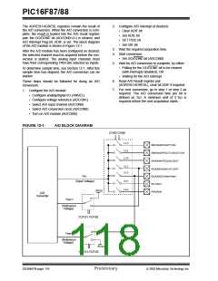
The Analog-to-Digital (A/D) converter module has
seven inputs for 18/20 pin devices (PIC16F88 devices
only).
The conversion of an analog input signal results in a
corresponding 10-bit digital number. The A/D module
has a high and low voltage reference input that is soft-
ware selectable to some combination of VDD, VSS,
VREF- (RA2), or VREF+ (RA3).
The ADCON0 register, shown in Register 12-2, con-
trols the operation of the A/D module. The ANSEL reg-
ister, shown in Register 12-1 and the ADCON1 register,
shown in Register 12-3, configure the functions of the
port pins. The port pins can be configured as analog
inputs (RA3/RA2 can also be voltage references) or as
digital I/O.
The A/D converter has a unique feature of being able
to operate while the device is in SLEEP mode. To oper-
ate in SLEEP, the A/D conversion clock must be
derived from the A/D’s internal RC oscillator.
Additional information on using the A/D module can be
found in the PICmicro® Mid-Range MCU Family
Reference Manual (DS33023).
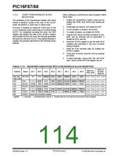
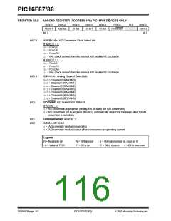
REGISTER 12-1: ANSEL REGISTER (ADDRESS 9Bh) PIC16F88 DEVICES ONLY
U-0
—
R/W-1
ANS6
R/W-1
ANS5
R/W-1
ANS4
R/W-1
ANS3
R/W-1
ANS2
R/W-1
ANS1
R/W-1
ANS0
bit 7
bit 0
bit 7
Unimplemented: Read as ‘0’
bit 6-0 ANS<6:0>: Analog Input Select bits
Bits select input function on corresponding AN<6:0> pins.
1= Analog I/O (see notes below)
0= Digital I/O
Note 1: Setting a pin to an analog input disables the digital input buffer. The corresponding
TRIS bit should be set to input mode when using pins as analog inputs. Only AN2 is
an analog I/O, all other ANx pins are analog inputs.
2: See the block diagrams for the analog I/O pins to see how ANSEL interacts with the
CHS bits of the ADCON0 register.
Legend:
R = Readable bit
-n = Value at POR
W = Writable bit
‘1’ = Bit is set
U = Unimplemented bit, read as ‘0’
‘0’ = Bit is cleared x = Bit is unknown
2003 Microchip Technology Inc.
Preliminary
DS30487B-page 113

 MICROCHIP [ MICROCHIP ]