PIC16F/LF1946/47
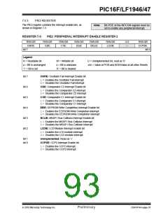
7.5.3
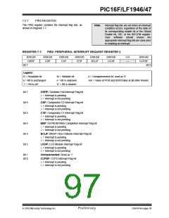
PIE2 REGISTER
The PIE2 register contains the interrupt enable bits, as
shown in Register 7-3.
Note:
Bit PEIE of the INTCON register must be
set to enable any peripheral interrupt.
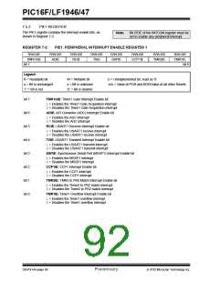
REGISTER 7-3:
PIE2: PERIPHERAL INTERRUPT ENABLE REGISTER 2
R/W-0/0
OSFIE
bit 7
R/W-0/0
C2IE
R/W-0/0
C1IE
R/W-0/0
EEIE
R/W-0/0
BCLIE
R/W-0/0
LCDIE
U-0
—
R/W-0/0
CCP2IE
bit 0
Legend:
R = Readable bit
W = Writable bit
U = Unimplemented bit, read as ‘0’
-n/n = Value at POR and BOR/Value at all other Resets
u = Bit is unchanged
‘1’ = Bit is set
x = Bit is unknown
‘0’ = Bit is cleared
bit 7
bit 6
bit 5
bit 4
bit 3
bit 2
OSFIE: Oscillator Fail Interrupt Enable bit
1= Enables the Oscillator Fail interrupt
0= Disables the Oscillator Fail interrupt
C2IE: Comparator C2 Interrupt Enable bit
1= Enables the Comparator C2 interrupt
0= Disables the Comparator C2 interrupt
C1IE: Comparator C1 Interrupt Enable bit
1= Enables the Comparator C1 interrupt
0= Disables the Comparator C1 interrupt
EEIE: EEPROM Write Completion Interrupt Enable bit
1= Enables the EEPROM Write Completion interrupt
0= Disables the EEPROM Write Completion interrupt
BCLIE: MSSP1 Bus Collision Interrupt Enable bit
1= Enables the MSSP1 Bus Collision Interrupt
0= Disables the MSSP1 Bus Collision Interrupt
LCDIE: LCD Module Interrupt Enable bit
1= Enables the LCD module interrupt
0= Disables the LCD module interrupt
bit 1
bit 0
Unimplemented: Read as ‘0’
CCP2IE: CCP2 Interrupt Enable bit
1= Enables the CCP2 interrupt
0= Disables the CCP2 interrupt
2010 Microchip Technology Inc.
Preliminary
DS41414A-page 91

 MICROCHIP [ MICROCHIP ]