PIC16F/LF1946/47
24.1.2
EUSART ASYNCHRONOUS
RECEIVER
24.1.2.2
Receiving Data
The receiver data recovery circuit initiates character
reception on the falling edge of the first bit. The first bit,
also known as the Start bit, is always a zero. The data
recovery circuit counts one-half bit time to the center of
the Start bit and verifies that the bit is still a zero. If it is
not a zero then the data recovery circuit aborts
character reception, without generating an error, and
resumes looking for the falling edge of the Start bit. If
the Start bit zero verification succeeds then the data
recovery circuit counts a full bit time to the center of the
next bit. The bit is then sampled by a majority detect
circuit and the resulting ‘0’ or ‘1’ is shifted into the RSR.
This repeats until all data bits have been sampled and
shifted into the RSR. One final bit time is measured and
the level sampled. This is the Stop bit, which is always
a ‘1’. If the data recovery circuit samples a ‘0’ in the
Stop bit position then a framing error is set for this
character, otherwise the framing error is cleared for this
character. See Section 24.1.2.5 “Receive Framing
Error” for more information on framing errors.
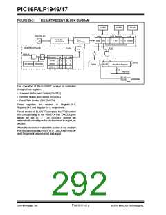
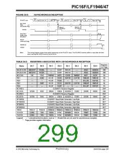
The Asynchronous mode would typically be used in
RS-232 systems. The receiver block diagram is shown
in Figure 24-2. The data is received on the RXx/DTx
pin and drives the data recovery block. The data
recovery block is actually
a high-speed shifter
operating at 16 times the baud rate, whereas the serial
Receive Shift Register (RSR) operates at the bit rate.
When all 8 or 9 bits of the character have been shifted
in, they are immediately transferred to a two character
First-In-First-Out (FIFO) memory. The FIFO buffering
allows reception of two complete characters and the
start of a third character before software must start
servicing the EUSART receiver. The FIFO and RSR
registers are not directly accessible by software.
Access to the received data is via the RCxREG
register.
24.1.2.1
Enabling the Receiver
The EUSART receiver is enabled for asynchronous
operation by configuring the following three control bits:
Immediately after all data bits and the Stop bit have
been received, the character in the RSR is transferred
to the EUSART receive FIFO and the RCxIF interrupt
flag bit of the PIR1/PIR3 register is set. The top charac-
ter in the FIFO is transferred out of the FIFO by reading
the RCxREG register.
• CREN = 1
• SYNC = 0
• SPEN = 1
All other EUSART control bits are assumed to be in
their default state.
Note:
If the receive FIFO is overrun, no additional
characters will be received until the overrun
condition is cleared. See Section 24.1.2.6
“Receive Overrun Error” for more
information on overrun errors.
Setting the CREN bit of the RCxSTA register enables
the receiver circuitry of the EUSART. Clearing the SYNC
bit of the TXxSTA register configures the EUSART for
asynchronous operation. Setting the SPEN bit of the
RCxSTA register enables the EUSART. The
programmer must set the corresponding TRIS bit to
configure the TX/CK I/O pin as an input.
24.1.2.3
Receive Data Polarity
The polarity of the receive data can be controlled with
the DTRXP bit of the BAUDxCON register. The default
state of this bit is ‘0’ which selects high true receive idle
and data bits. Setting the DTRXP bit to ‘1’ will invert the
receive data resulting in low true idle and data bits. The
DTRXP bit controls receive data polarity only in
Asynchronous mode. In synchronous mode the
DTRXP bit has a different function.
Note 1: If the RX/DT function is on an analog pin,
the corresponding ANSEL bit must be
cleared for the receiver to function.
If the RXx/DTx pin is shared with an analog peripheral
the analog I/O function must be disabled by clearing the
corresponding ANSEL bit.
DS41414A-page 294
Preliminary
2010 Microchip Technology Inc.

 MICROCHIP [ MICROCHIP ]