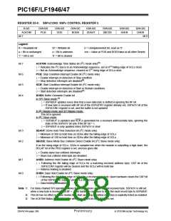
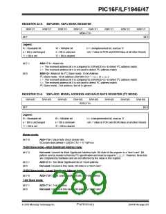
PIC16F/LF1946/47
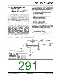
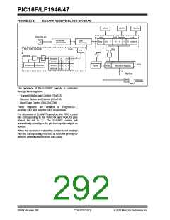
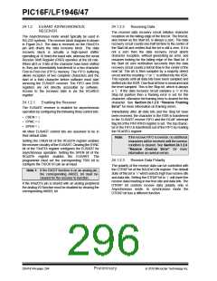
FIGURE 24-2:
EUSART RECEIVE BLOCK DIAGRAM
CREN
OERR
RCIDL
RXx/DTx pin
RSR Register
MSb
Stop (8)
LSb
0
START
Pin Buffer
and Control
Data
Recovery
7
1
• • •
Baud Rate Generator
FOSC
RX9
÷ n
BRG16
n
+ 1
Multiplier
x4
x16 x64
SYNC
BRGH
BRG16
1
X
1
1
0
1
0
0
0
1
0
0
0
FIFO
SPxBRGH SPxBRGL
X
X
RX9D
FERR
RCxREG Register
8
Data Bus
RCxIF
RCxIE
Interrupt
The operation of the EUSART module is controlled
through three registers:
• Transmit Status and Control (TXxSTA)
• Receive Status and Control (RCxSTA)
• Baud Rate Control (BAUDxCON)
These registers are detailed in Register 24-1,
Register 24-2 and Register 24-3, respectively.
For all modes of EUSART operation, the TRIS control
bits corresponding to the RXx/DTx and TXx/CKx pins
should be set to ‘1’. The EUSART control will
automatically reconfigure the pin from input to output, as
needed.
When the receiver or transmitter section is not enabled
then the corresponding RXx/DTx or TXx/CKx pin may be
used for general purpose input and output.
DS41414A-page 290
Preliminary
2010 Microchip Technology Inc.

 MICROCHIP [ MICROCHIP ]