PIC16F/LF1946/47
• Gate Toggle Mode
20.0 TIMER1 MODULE WITH GATE
CONTROL
• Gate Single-pulse Mode
• Gate Value Status
The Timer1 module is a 16-bit timer/counter with the
following features:
• Gate Event Interrupt
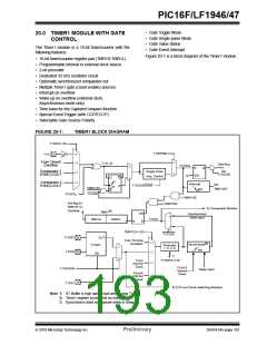
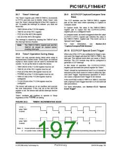
Figure 20-1 is a block diagram of the Timer1 module.
• 16-bit timer/counter register pair (TMR1H:TMR1L)
• Programmable internal or external clock source
• 2-bit prescaler
• Dedicated 32 kHz oscillator circuit
• Optionally synchronized comparator out
• Multiple Timer1 gate (count enable) sources
• Interrupt on overflow
• Wake-up on overflow (external clock,
Asynchronous mode only)
• Time base for the Capture/Compare function
• Special Event Trigger (with CCP/ECCP)
• Selectable Gate Source Polarity
FIGURE 20-1:
TIMER1 BLOCK DIAGRAM
T1GSS<1:0>
T1G
T1GSPM
00
From Timer0
Overflow
0
01
10
11
T1G_IN
D
Data Bus
T1GVAL
0
1
D
Q
Comparator 1
SYNCC1OUT
Single Pulse
Acq. Control
RD
1
T1GCON
Q1 EN
Q
Q
Comparator 2
SYNCC2OUT
Interrupt
Set
T1GGO/DONE
CK
R
TMR1ON
T1GTM
TMR1GIF
det
T1GPOL
TMR1GE
Set flag bit
TMR1IF on
Overflow
TMR1ON
To Comparator Module
TMR1(2)
EN
D
Synchronized
clock input
0
T1CLK
TMR1H
TMR1L
Q
1
TMR1CS<1:0>
T1SYNC
T1OSO
OUT
Cap. Sensing
Oscillator
11
10
Synchronize(3)
det
T1OSC
EN
Prescaler
1, 2, 4, 8
1
0
T1OSI
2
T1CKPS<1:0>
FOSC
Internal
Clock
01
00
FOSC/2
Internal
Clock
T1OSCEN
T1CKI
Sleep input
FOSC/4
Internal
Clock
(1)
To LCD and Clock Switching Modules
Note 1: ST Buffer is high speed type when using T1CKI.
2: Timer1 register increments on rising edge.
3: Synchronize does not operate while in Sleep.
2010 Microchip Technology Inc.
Preliminary
DS41414A-page 191

 MICROCHIP [ MICROCHIP ]