PIC16F/LF1946/47
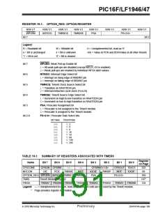
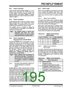
REGISTER 19-1: OPTION_REG: OPTION REGISTER
R/W-1/1
WPUEN
R/W-1/1
INTEDG
R/W-1/1
R/W-1/1
R/W-1/1
PSA
R/W-1/1
R/W-1/1
PS<2:0>
R/W-1/1
bit 0
TMR0CS
TMR0SE
bit 7
Legend:
R = Readable bit
W = Writable bit
U = Unimplemented bit, read as ‘0’
-n/n = Value at POR and BOR/Value at all other Resets
u = Bit is unchanged
‘1’ = Bit is set
x = Bit is unknown
‘0’ = Bit is cleared
bit 7
bit 6
bit 5
bit 4
bit 3
bit 2-0
WPUEN: Weak Pull-up Enable bit
1= All weak pull-ups are disabled (except MCLR, if it is enabled)
0= Weak pull-ups are enabled by individual WPUx latch values
INTEDG: Interrupt Edge Select bit
1= Interrupt on rising edge of RB0/INT pin
0= Interrupt on falling edge of RB0/INT pin
TMR0CS: Timer0 Clock Source Select bit
1= Transition on RA4/T0CKI pin
0= Internal instruction cycle clock (FOSC/4)
TMR0SE: Timer0 Source Edge Select bit
1= Increment on high-to-low transition on RA4/T0CKI pin
0= Increment on low-to-high transition on RA4/T0CKI pin
PSA: Prescaler Assignment bit
1= Prescaler is not assigned to the Timer0 module
0= Prescaler is assigned to the Timer0 module
PS<2:0>: Prescaler Rate Select bits
Bit Value
Timer0 Rate
000
001
010
011
100
101
110
111
1 : 2
1 : 4
1 : 8
1 : 16
1 : 32
1 : 64
1 : 128
1 : 256
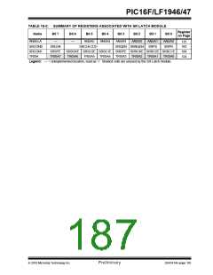
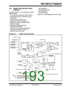
TABLE 19-1: SUMMARY OF REGISTERS ASSOCIATED WITH TIMER0
Register
on Page
Name
Bit 7
Bit 6
Bit 5
Bit 4
Bit 3
Bit 2
Bit 1
Bit 0
CPSCON0
INTCON
CPSON CPSRM
GIE PEIE
—
—
CPSRNG<1:0>
CPSOUT T0XCS
323
89
TMR0IE
INTE
IOCIE
PSA
TMR0IF
INTF
IOCIF
OPTION_REG WPUEN INTEDG TMR0CS TMR0SE
PS<2:0>
189
187*
124
TMR0
TRISA
Timer0 Module Register
TRISA7 TRISA6 TRISA5 TRISA4
TRISA3
TRISA2
TRISA1 TRISA0
Legend: — = Unimplemented location, read as ‘0’. Shaded cells are not used by the Timer0 module.
Page provides register information.
*
2010 Microchip Technology Inc.
Preliminary
DS41414A-page 189

 MICROCHIP [ MICROCHIP ]