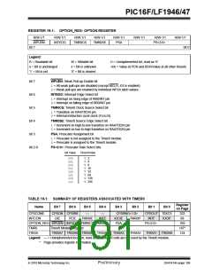
PIC16F/LF1946/47
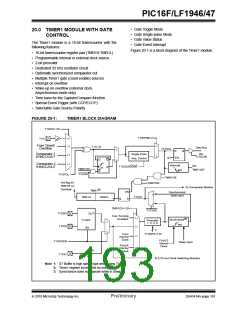
20.3 Timer1 Prescaler
20.6 Timer1 Gate
Timer1 has four prescaler options allowing 1, 2, 4 or 8
divisions of the clock input. The T1CKPS bits of the
T1CON register control the prescale counter. The
prescale counter is not directly readable or writable;
however, the prescaler counter is cleared upon a write to
TMR1H or TMR1L.
Timer1 can be configured to count freely or the count
can be enabled and disabled using Timer1 Gate
circuitry. This is also referred to as Timer1 Gate Enable.
Timer1 Gate can also be driven by multiple selectable
sources.
20.6.1
TIMER1 GATE ENABLE
20.4 Timer1 Oscillator
The Timer1 Gate Enable mode is enabled by setting
the TMR1GE bit of the T1GCON register. The polarity
of the Timer1 Gate Enable mode is configured using
the T1GPOL bit of the T1GCON register.
A dedicated low-power 32.768 kHz oscillator circuit is
built-in between pins T1OSI (input) and T1OSO
(amplifier output). This internal circuit is to be used in
conjunction with an external 32.768 kHz crystal.
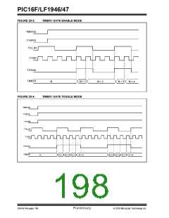
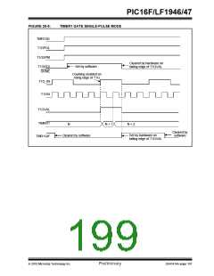
When Timer1 Gate Enable mode is enabled, Timer1
will increment on the rising edge of the Timer1 clock
source. When Timer1 Gate Enable mode is disabled,
no incrementing will occur and Timer1 will hold the
current count. See Figure 20-3 for timing details.
The oscillator circuit is enabled by setting the
T1OSCEN bit of the T1CON register. The oscillator will
continue to run during Sleep.
Note:
The oscillator requires a start-up and
stabilization time before use. Thus,
T1OSCEN should be set and a suitable
delay observed prior to enabling Timer1.
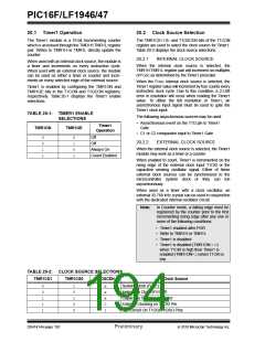
TABLE 20-3: TIMER1 GATE ENABLE
SELECTIONS
T1CLK T1GPOL
T1G
Timer1 Operation
20.5 Timer1 Operation in
Asynchronous Counter Mode
0
0
1
1
0
1
0
1
Counts
Holds Count
Holds Count
Counts
If control bit T1SYNC of the T1CON register is set, the
external clock input is not synchronized. The timer
increments asynchronously to the internal phase
clocks. If the external clock source is selected then the
timer will continue to run during Sleep and can
generate an interrupt on overflow, which will wake-up
the processor. However, special precautions in
software are needed to read/write the timer (see
Section 20.5.1 “Reading and Writing Timer1 in
Asynchronous Counter Mode”).
20.6.2
TIMER1 GATE SOURCE
SELECTION
The Timer1 Gate source can be selected from one of
four different sources. Source selection is controlled by
the T1GSS bits of the T1GCON register. The polarity
for each available source is also selectable. Polarity
selection is controlled by the T1GPOL bit of the
T1GCON register.
Note:
When switching from synchronous to
asynchronous operation, it is possible to
skip an increment. When switching from
asynchronous to synchronous operation,
it is possible to produce an additional
increment.
TABLE 20-4: TIMER1 GATE SOURCES
T1GSS
Timer1 Gate Source
Timer1 Gate Pin
00
01
Overflow of Timer0
20.5.1
READING AND WRITING TIMER1 IN
ASYNCHRONOUS COUNTER
MODE
(TMR0 increments from FFh to 00h)
10
11
Comparator 1 Output SYNCC1OUT
(optionally Timer1 synchronized output)
Reading TMR1H or TMR1L while the timer is running
from an external asynchronous clock will ensure a valid
read (taken care of in hardware). However, the user
should keep in mind that reading the 16-bit timer in two
8-bit values itself, poses certain problems, since the
timer may overflow between the reads.
Comparator 2 Output SYNCC2OUT
(optionally Timer1 synchronized output)
For writes, it is recommended that the user simply stop
the timer and write the desired values. A write
contention may occur by writing to the timer registers,
while the register is incrementing. This may produce an
unpredictable value in the TMR1H:TMR1L register pair.
2010 Microchip Technology Inc.
Preliminary
DS41414A-page 193

 MICROCHIP [ MICROCHIP ]