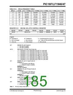
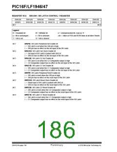
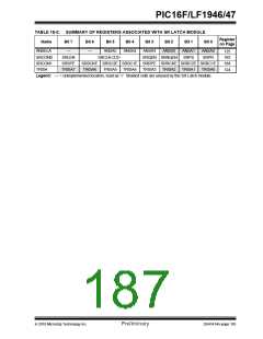
PIC16F/LF1946/47
When TMR0 is written, the increment is inhibited for
two instruction cycles immediately following the write.
19.0 TIMER0 MODULE
The Timer0 module is an 8-bit timer/counter with the
following features:
Note:
The value written to the TMR0 register can
be adjusted, in order to account for the two
instruction cycle delay when TMR0 is
written.
• 8-bit timer/counter register (TMR0)
• 8-bit prescaler (independent of Watchdog Timer)
• Programmable internal or external clock source
• Programmable external clock edge selection
• Interrupt on overflow
19.1.2
8-BIT COUNTER MODE
In 8-Bit Counter mode, the Timer0 module will increment
on every rising or falling edge of the T0CKI pin or the
Capacitive Sensing Oscillator (CPSCLK) signal.
• TMR0 can be used to gate Timer1
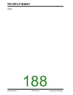
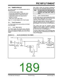
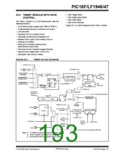
Figure 19-1 is a block diagram of the Timer0 module.
8-Bit Counter mode using the T0CKI pin is selected by
setting the TMR0CS bit in the OPTION register to ‘1’
and resetting the T0XCS bit in the CPSCON0 register to
‘0’.
19.1 Timer0 Operation
The Timer0 module can be used as either an 8-bit timer
or an 8-bit counter.
8-Bit Counter mode using the Capacitive Sensing
Oscillator (CPSCLK) signal is selected by setting the
TMR0CS bit in the OPTION register to ‘1’ and setting
the T0XCS bit in the CPSCON0 register to ‘1’.
19.1.1
8-BIT TIMER MODE
The Timer0 module will increment every instruction
cycle, if used without a prescaler. 8-Bit Timer mode is
selected by clearing the TMR0CS bit of the OPTION
register.
The rising or falling transition of the incrementing edge
for either input source is determined by the TMR0SE bit
in the OPTION register.
FIGURE 19-1:
BLOCK DIAGRAM OF THE TIMER0
FOSC/4
Data Bus
0
1
8
T0CKI
1
Sync
0
1
TMR0
2 TCY
0
Set Flag bit TMR0IF
From CPSCLK
on Overflow
TMR0CS
TMR0SE
8-bit
Prescaler
PSA
Overflow to Timer1
T0XCS
8
PS<2:0>
2010 Microchip Technology Inc.
Preliminary
DS41414A-page 187

 MICROCHIP [ MICROCHIP ]