PIC16F/LF1946/47
17.7 Comparator Negative Input
Selection
17.10 Analog Input Connection
Considerations
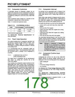
The CxNCH<1:0> bits of the CMxCON0 register direct
one of four analog pins to the comparator inverting
input.
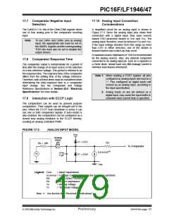
A simplified circuit for an analog input is shown in
Figure 17-3. Since the analog input pins share their
connection with a digital input, they have reverse
biased ESD protection diodes to VDD and VSS. The
analog input, therefore, must be between VSS and VDD.
If the input voltage deviates from this range by more
than 0.6V in either direction, one of the diodes is
forward biased and a latch-up may occur.
Note:
To use CxIN+ and CxINx- pins as analog
input, the appropriate bits must be set in
the ANSEL register and the corresponding
TRIS bits must also be set to disable the
output drivers.
A maximum source impedance of 10 k is recommended
for the analog sources. Also, any external component
connected to an analog input pin, such as a capacitor or
a Zener diode, should have very little leakage current to
minimize inaccuracies introduced.
17.8 Comparator Response Time
The comparator output is indeterminate for a period of
time after the change of an input source or the selection
of a new reference voltage. This period is referred to as
the response time. The response time of the comparator
differs from the settling time of the voltage reference.
Therefore, both of these times must be considered when
determining the total response time to a comparator
input change. See the Comparator and Voltage
Reference Specifications in Section 29.0 “Electrical
Specifications” for more details.
Note 1: When reading a PORT register, all pins
configured as analog inputs will read as a
‘0’. Pins configured as digital inputs will
convert as an analog input, according to
the input specification.
2: Analog levels on any pin defined as a
digital input, may cause the input buffer to
consume more current than is specified.
17.9 Interaction with ECCP Logic
The comparators can be used as general purpose
comparators. Their outputs can be brought out to the
pins. When the ECCP Auto-Shutdown is active it can
use one or both comparator signals. If auto-restart is
also enabled, the comparators can be configured as a
closed loop analog feedback to the ECCP, thereby,
creating an analog controlled PWM.
FIGURE 17-3:
ANALOG INPUT MODEL
VDD
Analog
Input
pin
VT 0.6V
RIC
Rs < 10K
To Comparator
(1)
ILEAKAGE
CPIN
5 pF
VA
VT 0.6V
Vss
Legend: CPIN
= Input Capacitance
ILEAKAGE = Leakage Current at the pin due to various junctions
RIC
RS
VA
= Interconnect Resistance
= Source Impedance
= Analog Voltage
VT
= Threshold Voltage
Note 1: See Section 29.0 “Electrical Specifications”.
2010 Microchip Technology Inc.
Preliminary
DS41414A-page 177

 MICROCHIP [ MICROCHIP ]